This article provides an overview of STM32MP157x-DKx Discovery kits.
1. Article purpose[edit | edit source]
This article briefly describes:
- what are the different components present on the board
- how to connect the board to external material
- how to configure the board for boot
- what are the configurations of the connector pins
This article is valid for the STM32MP157A-DK1 ![]() [1], STM32MP157D-DK1
[1], STM32MP157D-DK1 ![]() [2], STM32MP157C-DK2
[2], STM32MP157C-DK2 ![]() [3] and STM32MP157F-DK2
[3] and STM32MP157F-DK2 ![]() [4] Discovery kits: the part numbers are specified in the STM32MP15 microprocessor part numbers article.
[4] Discovery kits: the part numbers are specified in the STM32MP15 microprocessor part numbers article.
2. Board assembly[edit | edit source]
The STM32MP157x-DKx Discovery kits packages (STM32MP157A-DK1 ![]() , STM32MP157D-DK1
, STM32MP157D-DK1 ![]() , STM32MP157C-DK2
, STM32MP157C-DK2 ![]() and STM32MP157F-DK2
and STM32MP157F-DK2 ![]() ) are delivered assembled, and contain the items listed below. A USB Type-C™ cable is also included.
) are delivered assembled, and contain the items listed below. A USB Type-C™ cable is also included.
Please note that;
- the STM32MP157A-DK1
 and STM32MP157D-DK1
  Discovery kits neither include the "WLAN + Bluetooth" component (muRata LBEE5KL1DX), nor the MB1407 daughterboard DSI display
 - the STM32MP157C-DK2 and STM32MP157F-DK2 Discovery kits include the "WLAN + Bluetooth" component (muRata LBEE5KL1DX), and the MB1407 daughterboard DSI display
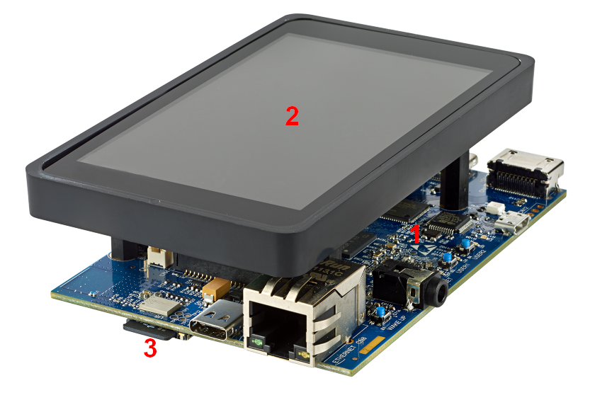
| Position | Description |
|---|---|
| 1 | MB1272 motherboard ("WLAN + Bluetooth" component included only for the STM32MP157C-DK2 |
| 2 | MB1407 daughterboard DSI display (480x800 pixels): only for the STM32MP157C-DK2 |
| 3 | microSD card |
3. Board overview[edit | edit source]
| Position | Description |
|---|---|
| 1 | MB1272 motherboard |
| 2 | MB1407 daughterboard DSI display (480x800 pixels): only for the STM32MP157C-DK2 |
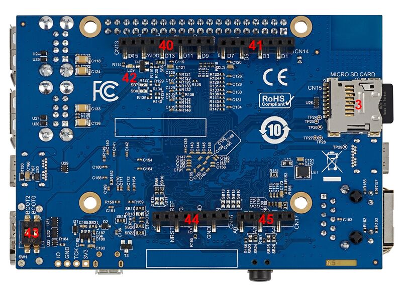
| 3 (CN15) | microSD card |
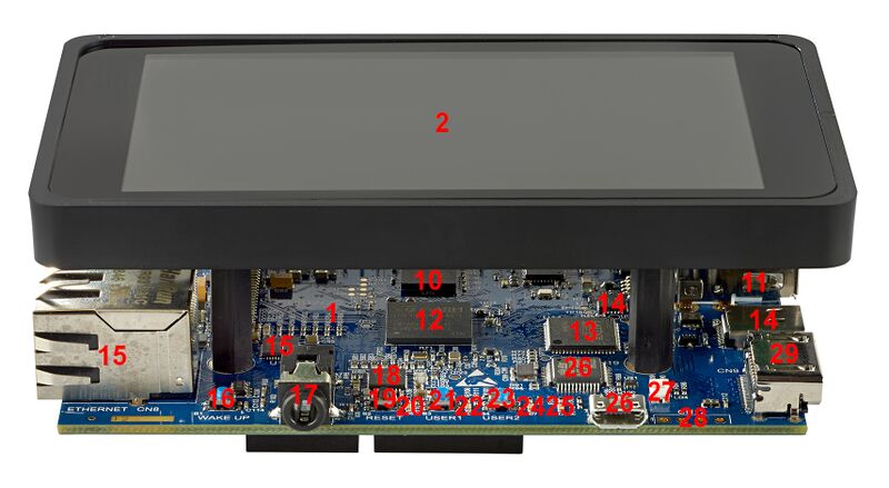
| Position | Description | Position | Description |
|---|---|---|---|
| 10 (U5) | DDR3L 16 bits | 11 (CN5) | 2 USB Type-A (host) |
| 12 (U13) | STM32MP157x 12x12 | 13 (U14) | HDMI |
| 14 (CN7 and U12) | USB Type-C (DRP) | 15 (CN8 and (U18) | Ethernet |
| 16 (B1) | Wakeup button | 17 (CN10) | Audio headset |
| 18 (U20) | Audio codec (Cirrus CS42L51) | 19 (B2) | Reset button |
| 20 (LD5) | User LED (green)[LEDs 1] | 21 (B3) | User button (USER1) |
| 22 (LD6) | User LED (red)[LEDs 1] | 23 (B4) | User button (USER2) |
| 24 (LD7) | User LED (orange)[LEDs 1] | 25 (LD8) | User LED (blue)[LEDs 1] |
| 26 (CN11 and U19) | USB micro-B (ST-LINK/V2-1) | 27 (LD4) | ST-LINK/V2-1 LED (bicolor)[LEDs 2] |
| 28 ('CN12) | ST-LINK/V2-1 DFU | 29 (CN9) | HDMI connector |
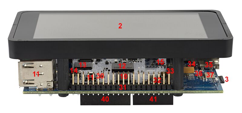
| Position | Description | Position | Description |
|---|---|---|---|
| 10 (U5) | DDR3L 16 bits | 11 (CN5 and U7) | 2 USB Type-A (host) |
| 12 (U13) | STM32MP157x 12x12 | 13 (U14) | HDMI |
| 14 (CN7 and U12) | USB Type-C (DRP) | 15 (CN8 and (U18) | Ethernet |
| 30 (LD1) | USB Type-A LED (red)[LEDs 3] | 31 (CN2) | GPIO expansion |
| 32 (U4) | PMIC (STPMIC1A) | 33 (CN4) | DSI LCD connector |
| 34 (LD3) | Ethernet LED (green)[LEDs 4] | 35 (CN6) | USB Type-C (power 5V-3A) |
| 36 (LD2) | Power LED (green)[LEDs 5] | 37 (U8) | WLAN + Bluetooth (muRata LBEE5KL1DX): only for STM32MP157C-DK2 |
| 40 (CN13) | Arduino Uno connector (socket 10x1) | 41 (CN14) | Arduino Uno connector (socket 8x1) |
| Position | Description | Position | Description |
|---|---|---|---|
| 40 (CN13) | Arduino Uno connector (socket 10x1) | 41 (CN14) | Arduino Uno connector (socket 8x1) |
| 42 (LD9) | Arduino LED (green) | 43 (SW1) | Boot mode selection |
| 44 (CN16) | Arduino Uno connector (socket 8x1) | 45 (CN17) | Arduino Uno connector (socket 6x1) |
Details about some LEDs:
- ↑ 1.0 1.1 1.2 1.3 LD5, LD6, LD7, LD8: some user LEDs are used to reflect the system activity, while the others are left free to be used by the application, as explained in LEDs and buttons on STM32 MPU boards article
- ↑ LD4: flashes red if ST-LINK/V2-1 connection not established, else green
- ↑ LD1: turns red if USB Type-A connection established
- ↑ LD3: flashes green when Ethernet connection established
- ↑ LD2: turns green if power connection established
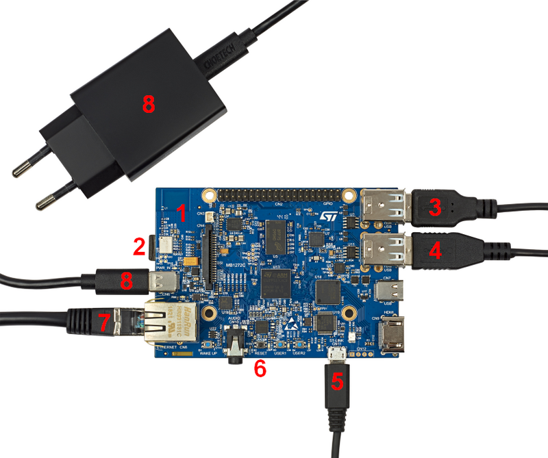
4. Board connection[edit | edit source]
The connections shown in the picture below are the ones recommended to start with the STM32MP157x_DKx Discovery kits. As shown in the board overview, other connectors are available for these boards (for example HDMI).
[edit | edit source]
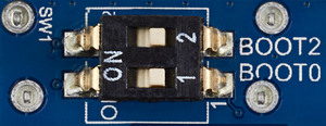
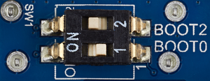
The following table defines the different combination of the boot mode selection switches based on ROM code selection:
| "Boot 1" is grounded (always 0) on the Discovery kits |
| Boot mode | Boot 0 | Boot 1 | Boot 2 |
|---|---|---|---|
| Forced USB boot for flashing |
0 | 0 | 0 |
| Not supported | 1 | 0 | 0 |
| Engineering boot | 0 | 0 | 1 |
| microSD card | 1 | 0 | 1 |
Below the corresponding configurations of the boot related switches (SW1 on the board overview picture):

6. GPIO mapping[edit | edit source]
6.1. GPIO expansion connector[edit | edit source]
The pins of the GPIO expansion connector (CN2 on the board overview picture) are described in the following table:
| Function | STM32 pin | Pin | Pin | STM32 pin | Function |
|---|---|---|---|---|---|
| 3V3 | - | 1 | 2 | - | 5V |
| GPIO2 / I2C5_SDA | PA12 | 3 | 4 | - | 5V |
| GPIO3 / I2C5_SCL | PA11 | 5 | 6 | - | GND |
| GPIO4 / MCO1 | PA8 | 7 | 8 | PB10 | GPIO14 / USART3_TX |
| GND | - | 9 | 10 | PB12 | GPIO15 / USART3_RX |
| GPIO17 / USART3_RTS | PG8 | 11 | 12 | PI5 | GPIO18 / SAI2_SCKA[EX 1] |
| GPIO27 / SDMMC3_D3 | PD7 | 13 | 14 | - | GND |
| GPIO22 / SDMMC3_CK | PG15 | 15 | 16 | PF1 | GPIO23 / SDMMC3_CMD |
| 3V3 | - | 17 | 18 | PF0 | GPIO24 / SDMMC3_D0 |
| GPIO10 / SPI5_MOSI | PF9 | 19 | 20 | - | GND |
| GPIO9 / SPI5_MISO | PF8 | 21 | 22 | PF4 | GPIO25 / SDMMC3_D1 |
| GPIO11 / SPI5_SCK | PF7 | 23 | 24 | PF6 | GPIO8 / SPI5_NSS |
| GND | - | 25 | 26 | PF3 | GPIO7 |
| I2C1_SDA[EX 2] | PF15 | 27 | 28 | PD12 | I2C1_SCL[EX 2] |
| GPIO5 / MCO2 | PG2 | 29 | 30 | - | GND |
| GPIO6 / TIM5_CH2 | PH11 | 31 | 32 | PD13 | GPIO12 / TIM4_CH2 |
| GPIO13 / TIM3_CH2 | PC7 | 33 | 34 | - | GND |
| GPIO19 / SAI2_FSA[EX 1] | PI7 | 35 | 36 | PB13 | GPIO16 / USART3_CTS |
| GPIO26 / SDMMC3_D2 | PF5 | 37 | 38 | PI6 | GPIO20 / SAI2_SDA[EX 1] |
| GND | - | 39 | 40 | PF11 | GPIO21 / SAI2_SDB[EX 1] |
- ↑ 1.0 1.1 1.2 1.3 The SAI2 is shared between the audio codec and the GPIO expansion connector. By default, the SAI2 is connected to the audio codec thanks to Solder Bridge SB13, SB14, SB15, and SB16: more details in the STM32MP157x-DKx Discovery kits user manuals.
- ↑ 2.0 2.1 Warning: the I2C1 is used to communicate with several on-board peripherals, but is also available on the GPIO expansion connector. So, it is important to ensure that new components added on the I2C1 connection will not disturb the bus behavior.
6.2. Arduino Uno connector[edit | edit source]
The pins of the Arduino Uno connector are described in the following table:
| Arduino Uno connector | |||||||||||||||||||||||||||||||||||||||||||||||||||||||||||||||||||||||||||||||||
|---|---|---|---|---|---|---|---|---|---|---|---|---|---|---|---|---|---|---|---|---|---|---|---|---|---|---|---|---|---|---|---|---|---|---|---|---|---|---|---|---|---|---|---|---|---|---|---|---|---|---|---|---|---|---|---|---|---|---|---|---|---|---|---|---|---|---|---|---|---|---|---|---|---|---|---|---|---|---|---|---|---|
|
| ||||||||||||||||||||||||||||||||||||||||||||||||||||||||||||||||||||||||||||||||
|
| ||||||||||||||||||||||||||||||||||||||||||||||||||||||||||||||||||||||||||||||||
6.3. User buttons and LEDs[edit | edit source]
The GPIO assignments for the user buttons and LEDs are described in the following table. Refer to LEDs and buttons on STM32 MPU boards article to get information on the functional mapping for each one.
| LED color and label | Button label | GPIO |
|---|---|---|
| Green LD5 (*) | USER1 (*) | PA14 |
| Red LD6 (*) | USER2 (*) | PA13 |
| Orange LD7 | - | PH7 |
| Blue LD8 | - | PD11 |
7. References[edit | edit source]