This article provides an overview of the STM32MP135F-DK ![]() Discovery kit.
Discovery kit.
1. Article purpose[edit | edit source]
This article briefly describes:
- what are the different components on the board
- how to connect the board to external material
- how to configure the board for boot
- what are the configurations of the connector pins
This article is valid for the STM32MP135F-DK ![]() [1] Discovery kit: the part numbers are specified in the STM32MP13 microprocessor part numbers article.
[1] Discovery kit: the part numbers are specified in the STM32MP13 microprocessor part numbers article.
2. Board assembly[edit | edit source]
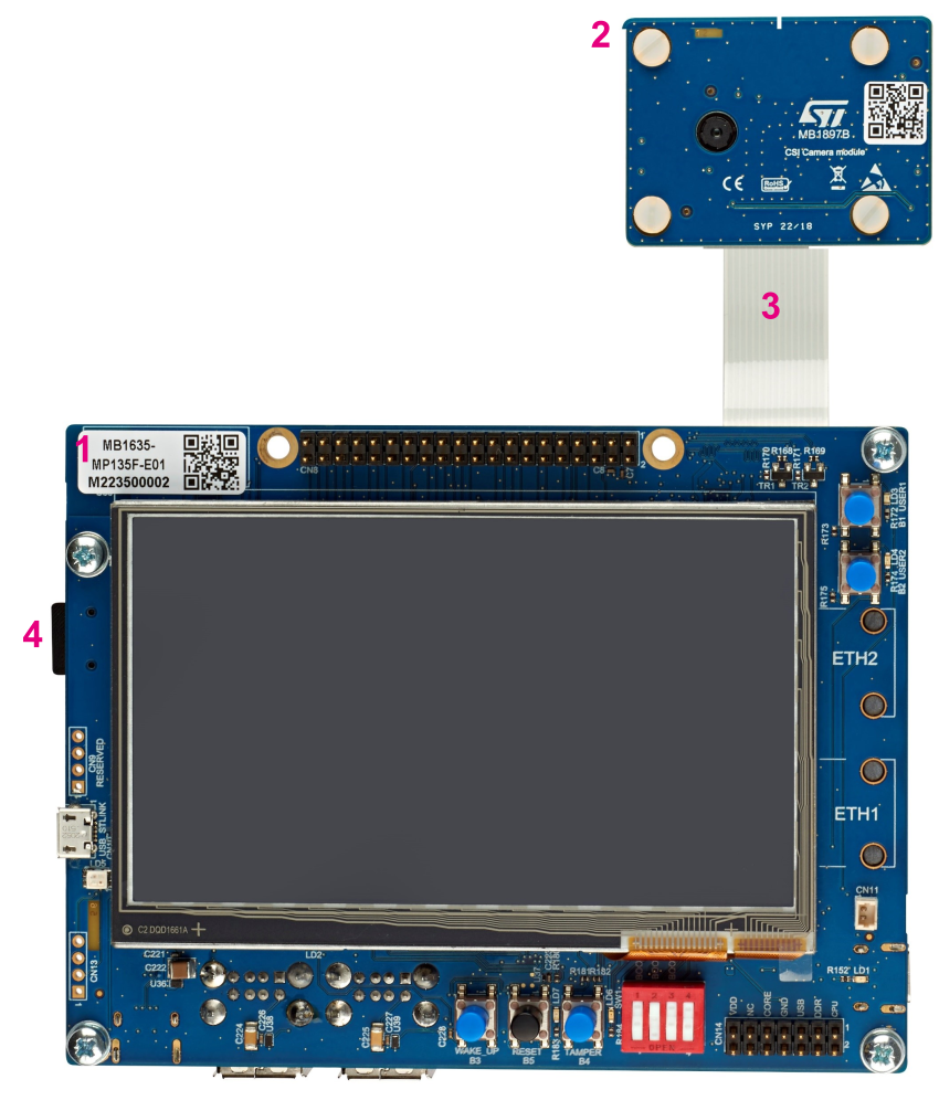
The STM32MP135F-DK Discovery kit ![]() package is composed of the items listed below.
package is composed of the items listed below.
| Position | Description |
|---|---|
| 1 | MB1635 mother board |
| 2 | MB1897 camera module (GalaxyCore GC2145 camera sensor) |
| 3 | Camera module flat cable |
| 4 | microSD™ card |
Note that the STM32MP135F-DK Discovery kit ![]() delivery does not contain a USB cable or a USB charger.
delivery does not contain a USB cable or a USB charger.
3. Board overview[edit | edit source]
| Position | Description | Position | Description |
|---|---|---|---|
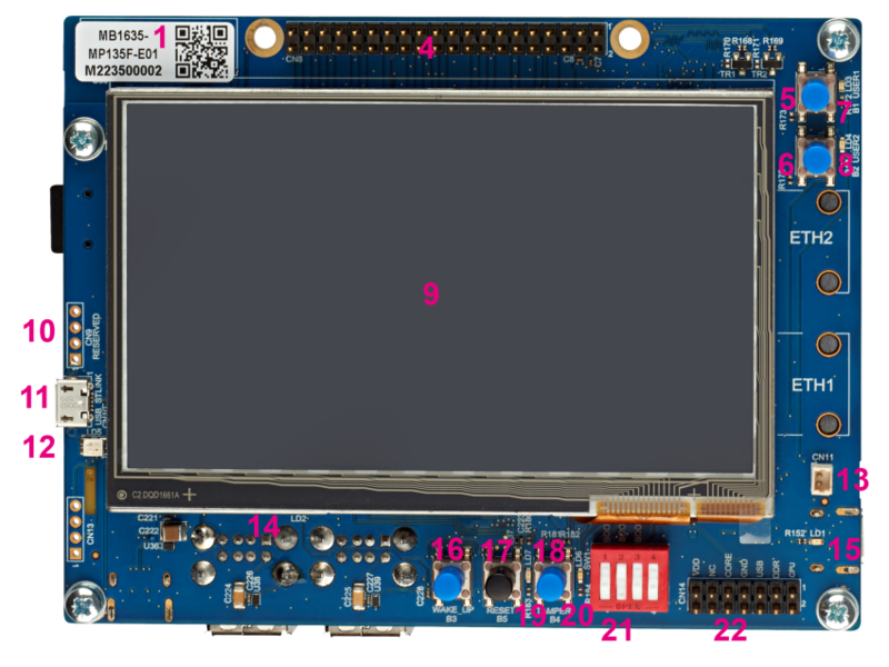
| 1 | MB1635 mother board | 4 (CN8) | GPIO expansion |
| 5 (B1) | User button (USER1) | 6 (B2) | User button (USER2) |
| 7 (LD3) | User LED (blue)[LEDs 1] | 8 (LD4) | User LED (red)[LEDs 1] |
| 9 (U35) | 4.3" LCD | 10 (CN9) | Reserved |
| 11 (CN10) | USB Micro-B (STLINK-V3E) | 12 (LD5) | STLINK-V3E LED (bicolor)[LEDs 2] |
| 13 (CN11) | Backup battery connector | 14 (LD2) | USB Type-A LED (red)[LEDs 3] |
| 15 (LD1) | Power LED (green) [LEDs 4] | 16 (B3) | Wake-up button |
| 17 (B5) | Reset button | 18 (B4) | Tamper button |
| 19 (LD7) | User LED (green) [LEDs 1] | 20 (LD6) | User LED (orange)[LEDs 1] |
| 21 (SW1) | Boot mode selection | 22 (CN14) | Power measurement connector |
| Position | Description | Position | Description |
|---|---|---|---|
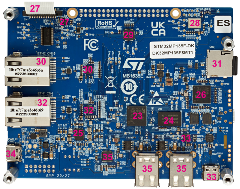
| 23 (U14) | STM32MP135F 11x11 | 24 (U17) | DDR3L 16 bits |
| 25 (U19) | PMIC (STPMIC1) | 26 (U12) | STLINK-V3E |
| 27 (CN1 and U2) | CSI-2 connector and bridge | 28 (U1) | WLAN + Bluetooth© (muRata LBEE5KL1DX) |
| 29 (U5) | 8-bit I/O expander | 30 (CN15 and U7) | Ethernet 2 |
| 31 (CN3) | microSD™ card connector | 32 (CN4 and U13) | Ethernet 1 |
| 33 (CN7 and U21) | USB Type-C© (flashload & DRP) via STM32G0 | 34 (CN12) | USB Type-C© (power 5V-3A) |
| 35 (CN5, CN6 and U33) | 2x dual USB Type-A (host) |
Details about some LEDs:
- ↑ 1.0 1.1 1.2 1.3 LD3, LD4, LD6, LD7: some user LEDs are used to reflect the system activity, while the others are left free for use by the application, as explained in the LEDs and buttons on STM32 MPU boards article
- ↑ LD5: flashes red if the STLINK-V3E connection is not established, green otherwise
- ↑ LD2: turns red if a USB Type-A connection is established
- ↑ LD1: turns green if the power connection established
4. Board connection[edit | edit source]
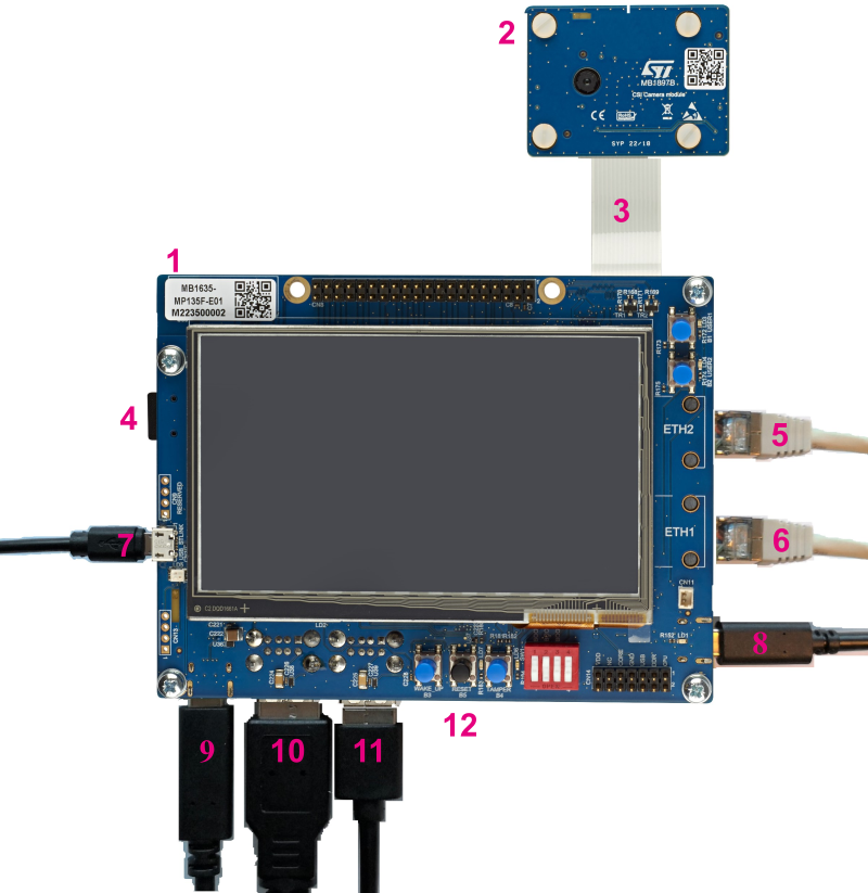
The connections shown in the picture below are the ones recommended to start with the STM32MP135x_DK Discovery kits. As shown in the board overview, other connectors are available for these boards (for example CSI-2).
[edit | edit source]
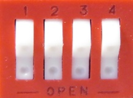
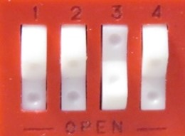
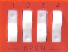
The following table defines the different combination of the boot mode selection switches based on ROM code selection:
| Boot mode | Boot 0 | Boot 1 | Boot 2 |
|---|---|---|---|
| USB/UART for programming |
0 | 0 | 0 |
| Engineering boot | 0 | 0 | 1 |
| microSD™ card | 1 | 0 | 1 |
| Not supported | Other codes | ||
| '0' is considered when switch is pushed in the OPEN position. It is ‘1’ otherwise. |
6. GPIO mapping[edit | edit source]
6.1. GPIO expansion connector[edit | edit source]
The pins of the GPIO expansion connector (CN8 on the board overview picture) are described in the following table:
| Function | STM32 pin | Pin | Pin | STM32 pin | Function |
|---|---|---|---|---|---|
| 3V3 | - | 1 | 2 | - | 5V |
| GPIO2 / I2C5_SDA[EX 1] | PH6 | 3 | 4 | - | 5V |
| GPIO3 / I2C5_SCL[EX 1] | PD1 | 5 | 6 | - | GND |
| GPIO4 / TIM3_CH4 | PB1 | 7 | 8 | PC0 | GPIO14 / USART1_TX |
| GND | - | 9 | 10 | PB0 | GPIO15 / USART1_RX |
| GPIO17 / USART1_RTS | PC2 | 11 | 12 | PA4 | GPIO18 / SAI1_SCKA |
| GPIO27 / DFSDM1_CKOUT | PC3 | 13 | 14 | - | GND |
| GPIO22 / DFSDM1_DATIN3 | PF13 | 15 | 16 | PG1 | GPIO23 / FDCAN2_TX |
| 3V3 | - | 17 | 18 | PG3 | GPIO24 / FDCAN2_RX |
| GPIO10 / SPI5_MOSI | PH3 | 19 | 20 | - | GND |
| GPIO9 / SPI5_MISO | PA8 | 21 | 22 | PI0 | GPIO25 / TAMP_IN8_OUT1 |
| GPIO11 / SPI5_SCK | PH7 | 23 | 24 | PH11 | GPIO8 / SPI5_NSS |
| GND | - | 25 | 26 | PF10 | GPIO7 |
| I2C1_SDA[EX 2] | PE8 | 27 | 28 | PD12 | I2C1_SCL[EX 2] |
| GPIO5 / MCO2 | PE6 | 29 | 30 | - | GND |
| GPIO6 / TIM4_CH2 | PD13 | 31 | 32 | PE5 | GPIO12 / TIM8_CH3 |
| GPIO13 / TIM14_CH1 | PF9 | 33 | 34 | - | GND |
| GPIO19 / SAI1_FSA | PF11 | 35 | 36 | PA7 | GPIO16 / USART1_CTS |
| GPIO26 / UART8_TX | PE1 | 37 | 38 | PA5 | GPIO20 / SAI1_SDA |
| GND | - | 39 | 40 | PA0 | GPIO21 / SAI1_SDB |
- ↑ 1.0 1.1 Warning: the I2C5 is used to communicate with several on-board peripherals but is also available on the GPIO expansion connector. So, it is important to ensure that new components added on the I2C5 connection do not disturb the bus behavior.
- ↑ 2.0 2.1 Warning: the I2C1 is used to communicate with several on-board peripherals but is also available on the GPIO expansion connector. So, it is important to ensure that new components added on the I2C1 connection will not disturb the bus behavior.
| No SDMMCx function is available on the GPIO expansion compared to the usual GPIO expansion connector. |
6.2. User buttons and LEDs[edit | edit source]
The GPIO assignments for the user buttons and LEDs are described in the following table. Refer to the article LEDs and buttons on STM32 MPU boards to get information on the functional mapping for each one.
| LED color and label | Button label | GPIO |
|---|---|---|
| Green LD7 (*) | - | MCP_IO4 |
| Red LD4 (*) | USER2 (*) | PA13 |
| Orange LD6 | - | MCP_IO5 |
| Blue LD3 | USER1 (*) | PA14 |
7. References[edit | edit source]