1. ROM code overview[edit source]
The ROM code is the first code executed by the Arm® Cortex®-A core(s) after application or system reset.
The main features of the ROM code are listed in the table below for each STM32MP1 series and STM32MP2 series processor:
| ROM code features | STM32MP13x lines |
STM32MP15x lines |
STM32MP25x lines | |
|---|---|---|---|---|
| STM32 header for FSBL loading | v2.0 | v1.0 | v2.2 | |
| Boot mode selection | Serial boot | |||
| Flash memory boot | ||||
| Developer (also known as "engineering") mode | ||||
| SSP (secure secrets provisioning) | ||||
| RMA (return material analysis) | done by BSEC HW | |||
| Image loading binary size (without STM32 header) | 128 KB | 247 KB | FSBLA: 247 KB FSBLM: 128 KB | |
| Secure boot | FSBL authentication (ECDSA) | |||
| FSBL authentication key revocation | ||||
| FSBL anti-rollback mechanism | ||||
| FSBL decryption (AES) | ||||
| Cryptographic accelerators (ECDSA, AES) | ||||
| Secondary core boot | ||||
| MCU cold boot | ||||
| MCU wake up boot | ||||
| Wake up from low power modes | ||||
| Secure services export | ||||
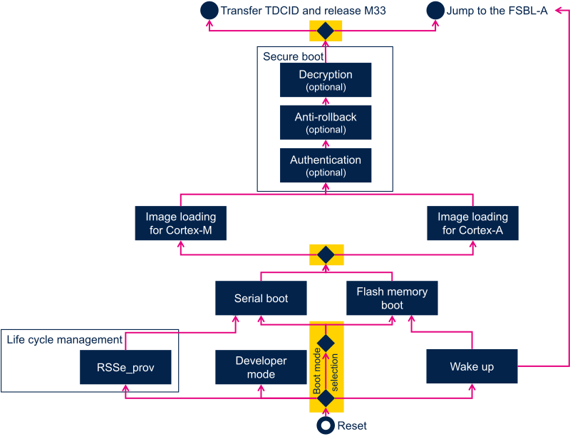
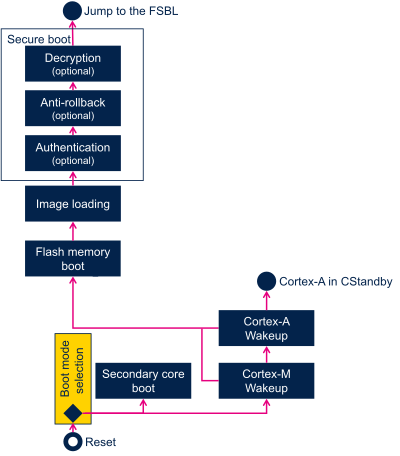
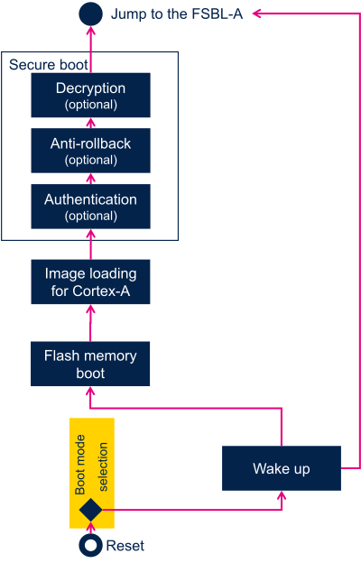
The diagram below puts these features in sequence. It illustrates the ROM code execution flow, and each step is further described in the following sections.
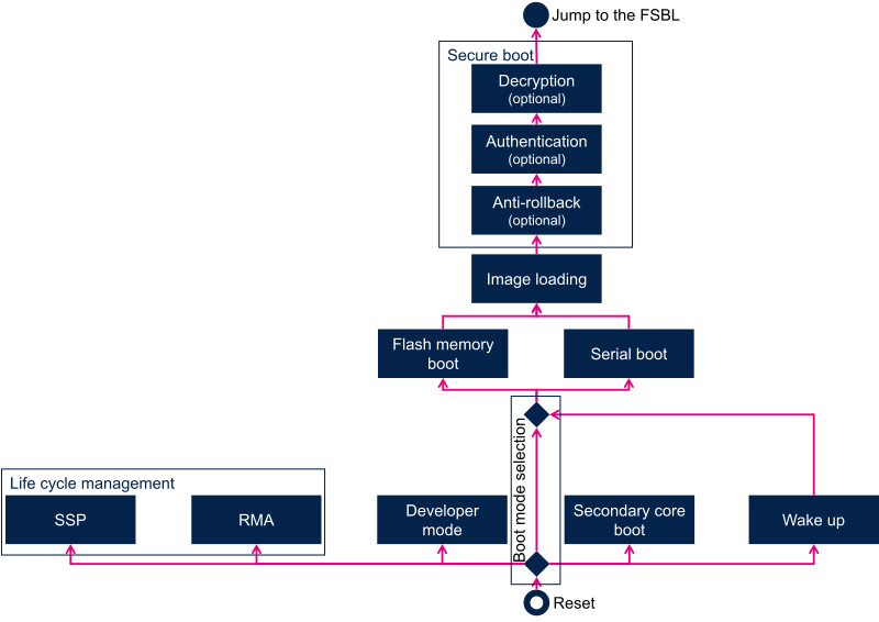
2. STM32 header[edit source]
To be properly recognized by the ROM code, the binary file loaded from the boot device must comply with a proprietary format, starting with a STM32 header.
The STM32MP15x lines ![]() complies with STM32 header v1.0, the STM32MP13x lines
complies with STM32 header v1.0, the STM32MP13x lines ![]() complies with STM32 header v2.0, and STM32MP25x lines
complies with STM32 header v2.0, and STM32MP25x lines ![]() uses the v2.2. The difference between these versions is mainly due to the introduction of the new secure boot features, listed in the previous section and described in the following ones.
uses the v2.2. The difference between these versions is mainly due to the introduction of the new secure boot features, listed in the previous section and described in the following ones.
3. Boot mode selection[edit source]
3.1. Boot device selection[edit source]
3.1.1. Boot device selection on STM32MP1 series[edit source]
As shown in the figure and table below, the boot mode is determined by the boot pin states, OTP words and one TAMP register.
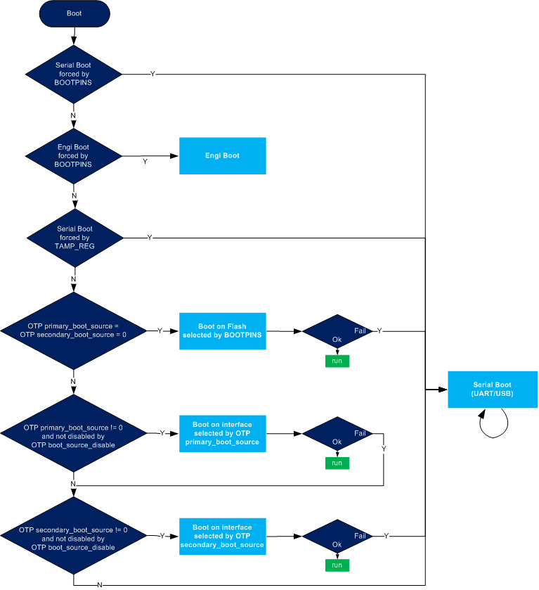
| BOOT pins | STM32MP13 TAMP_REG[30] STM32MP15 TAMP_REG[20] (Force Serial) |
Primary boot source | Secondary boot source | Boot source #1 | Boot source #2 if #1 fails |
Boot source if #2 fails |
|---|---|---|---|---|---|---|
| b000 (Force Serial) |
x (don't care) | x (don't care) | x (don't care) | Serial | - | - |
| b001 | != 0xFF | 0 (virgin) | 0 (virgin) | QSPI NOR | Serial | - |
| b010 | != 0xFF | 0 (virgin) | 0 (virgin) | e•MMC™ | Serial | - |
| b011 | != 0xFF | 0 (virgin) | 0 (virgin) | FMC NAND | Serial | - |
| b100 (DEV Boot) |
x (don't care) | x (don't care) | x (don't care) | NoBoot | - | - |
| b101 | != 0xFF | 0 (virgin) | 0 (virgin) | SD-Card | Serial | - |
| b110 | != 0xFF | 0 (virgin) | 0 (virgin) | Serial | - | - |
| b111 | != 0xFF | 0 (virgin) | 0 (virgin) | QSPI NAND | Serial | - |
| != b100 | != 0xFF | Primary1 | 0 (virgin) | Primary1 | Serial | - |
| != b100 | != 0xFF | 0 (virgin) | Secondary1 | Secondary1 | Serial | - |
| != b100 | != 0xFF | Primary1 | Secondary1 | Primary1 | Secondary1 | Serial |
| != b100 | 0xFF | x (don't care) | x (don't care) | Serial | - | - |
1Primary and Secondary are fields stored in OTP. When the selected boot mode is Serial boot or Flash memory boot, the ROM code configures the interface as specified in the following sub-sections. It loads the FSBL image into internal memory and runs Secure boot.
3.1.2. Boot device selection on STM32MP2 series[edit source]
As shown in the figure and table below, the boot mode is determined by boot pin states, OTP words and one TAMP register.
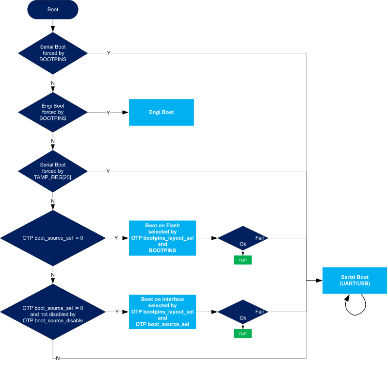

- Cortex-A35 master means that Cortex-A35 is the master of security. This mode is also called CA35 cold boot.
- Cortex-M33 master means that Cortex-M33 is the master of security. This mode is also called CM33 cold boot.
- Single device boot means that both FSBL-A and FSBL-M are stored on the same device,
- Dual device boot means that FSBL-A and FSBL-M are stored on different devices
Boot pins signification depends on the value of OTP bits selecting boot pins layout.
- 0b00 proposes most used configurations than can be used without blowing fuses,
| BOOT pins | Device selection | Cold boot processor | Dual mass storage support |
|---|---|---|---|
| b0000 | Serial link | Cortex-A35 | |
| b0001 | Cortex-A35 from SD-Card SDMMC1 | Cortex-A35 | |
| b0010 | Cortex-A35 from eMMC SDMMC2 | Cortex-A35 | |
| b0011 | Developer mode | na | |
| b0100 | Cortex-A35 from sNOR | Cortex-A35 | |
| b0101 | Cortex-A35 from sNAND | Cortex-A35 | |
| b0110 | Cortex-A35 from NAND FMC | Cortex-A35 | |
| b0111 | Cortex-M33 from SD-Card SDMMC1 | Cortex-M33 | |
| b1000 | Cortex-M33 from eMMC SDMMC2 | Cortex-M33 | |
| b1001 | Cortex-M33 from sNOR Cortex-A35 from sNAND |
Cortex-M33 | |
| b1010 | Cortex-M33 from sNOR Cortex-A35 from NAND FMC |
Cortex-M33 | |
| b1011 | Cortex-M33 from sNOR | Cortex-M33 | |
| b1100 | Developer mode | na | |
| b1101 | Cortex-M33 from sNOR Cortex-A35 from eMMC SDMMC2 |
Cortex-M33 | |
| b1110 | Cortex-M33 from sNOR Cortex-A35 from SD-Card SDMMC1 |
Cortex-M33 | |
| b1111 | Serial link | Cortex-A35 |
- 0b01 proposes only Cortex-A35 master, single device boot configurations,
| BOOT pins | Device selection | Cold boot processor | Dual mass storage support |
|---|---|---|---|
| b0000 | Serial link | Cortex-A35 | |
| b0001 | Cortex-A35 from SD-Card SDMMC1 | Cortex-A35 | |
| b0010 | Cortex-A35 from eMMC SDMMC2 | Cortex-A35 | |
| b0011 | Developer mode | na | |
| b0100 | Cortex-A35 from sNOR | Cortex-A35 | |
| b0101 | not used | - | - |
| b0110 | not used | - | - |
| b0111 | Cortex-A35 from Hyperflash | Cortex-A35 | |
| b1000 | Cortex-A35 from sNAND | Cortex-A35 | |
| b1001 | not used | - | - |
| b1010 | not used | - | - |
| b1011 | Cortex-A35 from NAND FMC | Cortex-A35 | |
| b1100 | Developer mode | na | |
| b1101 | Cortex-A35 from SD-Card SDMMC2 | Cortex-A35 | |
| b1110 | Cortex-A35 from eMMC SDMMC1 | Cortex-A35 | |
| b1111 | Serial link | Cortex-A35 |
- 0b10 proposes only Cortex-M33 master, single device boot configurations,
| BOOT pins | Device selection | Cold boot processor | Dual mass storage support |
|---|---|---|---|
| b0000 | Serial link | Cortex-A35 | |
| b0001 | Cortex-M33 from SD-Card SDMMC1 | Cortex-M33 | |
| b0010 | Cortex-M33 from eMMC SDMMC2 | Cortex-M33 | |
| b0011 | Developer mode | na | |
| b0100 | Cortex-M33 from sNOR | Cortex-M33 | |
| b0101 | not used | - | - |
| b0110 | not used | - | - |
| b0111 | Cortex-M33 from Hyperflash | Cortex-M33 | |
| b1000 | Cortex-M33 from sNAND | Cortex-M33 | |
| b1001 | not used | - | - |
| b1010 | not used | - | - |
| b1011 | Cortex-M33 from NAND FMC | Cortex-M33 | |
| b1100 | Developer mode | na | |
| b1101 | Cortex-M33 from SD-Card SDMMC2 | Cortex-M33 | |
| b1110 | Cortex-M33 from eMMC SDMMC1 | Cortex-M33 | |
| b1111 | Serial link | Cortex-A35 |
- 0b11 proposes only Cortex-M33 master, dual devices boot configurations,
| BOOT pins | Device selection | Cold boot processor | Dual mass storage support |
|---|---|---|---|
| b0000 | Serial link | Cortex-A35 | |
| b0001 | Cortex-M33 from sNOR Cortex-A35 from sNAND |
Cortex-M33 | |
| b0010 | Cortex-M33 from sNOR Cortex-A35 from eMMC SDMMC2 |
Cortex-M33 | |
| b0011 | Developer mode | na | |
| b0100 | Cortex-M33 from sNOR Cortex-A35 from NAND FMC |
Cortex-M33 | |
| b0101 | Cortex-M33 from sNOR Cortex-A35 from eMMC SDMMC1 |
Cortex-M33 | |
| b0110 | Cortex-M33 from Hyperflash Cortex-A35 from eMMC SDMMC1 |
Cortex-M33 | |
| b0111 | Cortex-M33 from Hyperflash Cortex-A35 from sNAND |
Cortex-M33 | |
| b1000 | Cortex-M33 from Hyperflash Cortex-A35 from eMMC SDMMC2 |
Cortex-M33 | |
| b1001 | Cortex-M33 from sNOR Cortex-A35 from SD-Card SDMMC2 |
Cortex-M33 | |
| b1010 | Cortex-M33 from Hyperflash Cortex-A35 from SD-Card SDMMC2 |
Cortex-M33 | |
| b1011 | Cortex-M33 from Hyperflash Cortex-A35 from NAND FMC |
Cortex-M33 | |
| b1100 | Developer mode | na | |
| b1101 | Cortex-M33 from sNOR Cortex-A35 from SD-Card SDMMC1 |
Cortex-M33 | |
| b1110 | Cortex-M33 from Hyperflash Cortex-A35 from SD-Card SDMMC1 |
Cortex-M33 | |
| b1111 | Serial link | Cortex-A35 |
Four special boot pin values are available whatever the boot pin layout is selected.
- 0b0000 and 0b1111 select serial boot,
- 0b0011 and 0b1100 select developer boot.
Boot source can be frozen by blowing OTP boot source selection with the selected boot pin values. In that case BootROM will no more care about boot pins values, except the four ones used for forcing serial boot or developer mode.
Serial boot can be forced through a backup register : BootROM looks for first backup register defined in the Zone3-RIF1 (read/write non-secure), if its value is 0xFF then it forces serial boot. See [RM] Section 74.3.8 for details.
Following table shows which image is loaded depending on the boot mode and the reset type.
| Reset type | Cold boot processor | |
|---|---|---|
| Cold boot A35 | Cold boot M33 | |
| Cold boot | load FSBL-A | load FSBL-M |
| Direct D1 DSTANDBY exit | load FSBL-A | load FSBL-A |
| D1 DSTANDBY exit following STANDBY exit | load FSBL-A | load FSBL-A |
| Simple D1 DSTANDBY exit with SYSRAM retention | No image loading. Direct jump to code in SYSRAM | No image loading. Direct jump to code in SYSRAM |
3.2. Serial boot[edit source]
The ROM code supports UART and USB serial interfaces.
When serial boot is selected, the ROM code scans, in parallel, all bootable UART instances and the USB. When activity is detected on an interface, the boot process proceeds with this interface and the others are ignored.
Note that it is possible to disable the USB or some UART instance by blowing relevant fuses of the boot source disable field in OTP. In all cases, whether the USB is disabled or not, HSE is mandatory.
3.2.1. USB boot[edit source]
3.2.1.1. USB boot on STM32MP1 series[edit source]
The ROM code supports boot on the USB OTG interface with HS PHY.
The ROM code uses OTG_HS_DP/DM signals available as additional functions on the USB_DP2/DM2 pins.
The USB OTG_HS is clocked by a 48 MHz and a 60 MHz clock, generated by using the HSE clock (from RCC).
The ROM code supports the following HSE values: 8, 10, 12, 14, 16, 20, 24, 25, 26, 28, 32, 36, 40, 48 MHz
The ROM code selects which HSE must be used by following these steps:
- if the disable HSE frequency autodetection OTP bit is set to 1, the ROM code considers HSE = 24 MHz.
- If the HSE value OTP field is 0b00 (default behavior), then the ROM code autodetects the HSE by using the HSI clock (from RCC).
- Recognized values are: 8, 10, 12, 14, 16, 20, 24, 32, 36, 28, 40, or 48 MHz.
- If none of these values are recognized, the ROM code considers that HSE = 24 MHz.
- Recognized values are: 8, 10, 12, 14, 16, 20, 24, 32, 36, 28, 40, or 48 MHz.
- If HSE value OTP field is 0b01, then it considers that HSE=24 MHz
- If HSE value OTP field is 0b10, then it considers that HSE=25 MHz
- If HSE value OTP field is 0b11, then it considers that HSE=26 MHz
3.2.1.2. USB boot on STM32MP2 series[edit source]
The ROM code supports boot on the USB3DR interface with USB2PHY2 in high speed mode.
The ROM code uses USB3DR interface in USB2 device mode.
The USB3DR is clocked by a 19.2, 20 or 24 Mhz clock, generated by using the HSE clock (from RCC).
The ROM code supports the following HSE values: 16, 19.2, 20, 24, 25, 26, 28, 32, 36, 40, 48 MHz
The ROM code selects which HSE must be used by following these steps:
- if the "disable HSE frequency autodetection" (see RM0457 table 34, "hse_frequency_autodetection_disable") OTP bit is set to 1, the ROM code considers HSE = 40 MHz.
- If the "HSE value" OTP field is 0b000 (default behavior), then the ROM code autodetects the HSE by using the HSI clock (from RCC).
- Recognized values are: 16, 20, 24, 28, 32, 36, 40 or 48 Mhz.
- If none of these values are recognized, the ROM code considers that HSE = 40 MHz.
- Recognized values are: 16, 20, 24, 28, 32, 36, 40 or 48 Mhz.
- If "HSE value" OTP field is 0b001, then it considers that HSE=24 MHz
- If "HSE value" OTP field is 0b010, then it considers that HSE=25 MHz
- If "HSE value" OTP field is 0b011, then it considers that HSE=26 MHz
- If "HSE value" OTP field is 0b100, then it considers that HSE=19.2 MHz
- If "HSE value" OTP field is 0b101, then it considers that HSE=40 MHz
- If "HSE value" OTP field is 0b110, then it considers that HSE=48 MHz
3.2.2. UART Boot[edit source]
The ROM code supports the following UART interfaces:
- USART/UART instances on STM32MP1 series:
- USART2, USART3, UART4, UART5, USART6, UART7, UART8
- USART/UART instances on STM32MP2 series:
- USART2, UART5, USART6, UART8, UART9
Configuration:
- (one start bit, 8 data bits, even parity bit and one stop bit).
By default the ROM code scans all UARTs listed above. This list may be reduced by blowing OTP fuses in UART instances disabling field.
In the case of serial boot, the ROM code applies the following AFmuxes.
The ROM code first muxes only the Rx pins of bootable UART instances, and scans all these Rx lines in parallel. When activity is detected on a UART interface, the ROM code muxes the related TX, all others Rx are unmuxed, and the boot process proceeds with this interface.
| STM32MP | Signal | GPIO pin and alternate function (AF) for | |||||||
|---|---|---|---|---|---|---|---|---|---|
| USART2 | USART3 | UART4 | UART5 | USART6 | UART7 | UART8 | UART9 | ||
| STM32MP15x lines |
RX | PA3 (AF07) | PB12 (AF08) | PB2 (AF08) | PB5 (MP15: AF12; MP13: AF11) |
PC7 (AF07) | PF6 (AF07) | PE0 (AF08) | |
| TX | PA2 (AF07) | PB10 (AF07) | PG11 (AF06) | PB13 (MP15: AF14; MP13: AF11) |
PC6 (AF07) | PF7 (AF07) | PE1 (AF08) | ||
| STM32MP13x lines |
RX | PB12 (AF08) | PD8 (AF08) | PB5 (AF12) | PC7 (AF07) | PF6 (AF07) | PE0 (AF08) | ||
| TX | PB10 (AF07) | PD6 (AF08) | PB13 (AF14) | PC6 (AF07) | PF7 (AF07) | PE1 (AF08) | |||
| STM32MP25x lines |
RX | PA8 (AF08) | PB15 (AF05) | PF4 (AF06) | PF3 (AF03) | PB14 (AF06) | |||
| TX | PA4 (AF06) | PA0 (AF05) | PF5 (AF06) | PG3 (AF03) | PD13 (AF06) | ||||
3.3. Flash memory boot[edit source]
The ROM code supports the following flash devices and interfaces:
| Flash device and interface | STM32MP13x lines |
STM32MP15x lines |
STM32MP25x lines | |
|---|---|---|---|---|
| serial NOR | via QUADSPI internal peripheral | |||
| via OCTOSPI internal peripheral | ||||
| serial NAND | flash via QUADSPI internal peripheral | |||
| via OCTOSPI internal peripheral | ||||
| parallel NAND | via FMC internal peripheral | |||
| Hyperflash | via OCTOSPI internal peripheral | |||
| SD card | via SDMMC internal peripheral | |||
| e•MMC™ | via SDMMC internal peripheral | |||
For more details on the mapping of each memory, refer to the STM32 MPU Flash mapping article.
3.3.1. Boot from parallel / serial NAND[edit source]
The NAND contains n copies of the FSBL in the first valid blocks. If the FSBL uses N blocks in the memory (N is usually 2 for a maximum 247 Kbyte FSBL with a memory having a 128 Kbyte block size), the ROM code scans blocks from the first and looks for the FSBL in the first N consecutive valid blocks found.
The ROM code supports parallel (via FMC) NAND and serial (via QSPI) NAND.
Supported parallel NAND:
The ROM code supports parallel NAND with the following parameters.
| Block size (KBytes ) |
Page size (KBytes) |
Data width | ECC1(bits and code) |
|---|---|---|---|
| 128 | 2 | 8, 16 | 4 (bch), 8 (bch), 1 (hamming) |
| 256 | 4 | 8, 16 | 4 (bch), 8 (bch), 1 (hamming) |
| 512 | 4 | 8, 16 | 4 (bch), 8 (bch), 1 (hamming) |
| 512 | 8 | 8, 16 | 4 (bch), 8 (bch), 1 (hamming) |
- 1: The ROM code supports both parallel NAND with or without on-die ECC. The ECC given here is for NAND without on-die ECC.
Supported serial NAND:
The ROM code supports serial NAND with the following parameters.
| Block size (KBytes) |
Page size (KBytes) |
|---|---|
| 128 | 2 |
| 256 | 4 |
| 512 | 4 |
| 512 | 8 |
The ROM code only supports serial NAND with embedded ECC.
Some serial NANDs are multi-plane. The ROM code supports such multi-plane features when the OTP bit serial NAND plane selection is set to 1.
Configuration:
In order to read a NAND flash memory, the ROM code needs to know the page size, the block size and the number of blocks. For parallel NAND, it also needs to know the width and the number of ECC bits.
The ROM code detects the NAND-parameter storage location by checking nand param stored in otp OTP bit value.
If the nand param stored in otp OTP bit value is equal to 0 (which is the default), the NAND must provide an ONFI compatible parameter table in which the ROM code looks for NAND parameters. “ONFI compatible ” means that the NAND provides a get parameter feature that returns a table where parameters needed by ROM code are located at standard ONFI offsets.
If the nand param stored in otp OTP bit value is equal to 1, the ROM code looks for the NAND parameter in OTP.
The number of ECC bits is a particular case, as it can be set by OTP even if the nand param stored in otp is equal to 0. This is to allow the user to override the recommended number of ECC bits given by the parameter table of an ONFI NAND.
Note that serial NANDs are neither ONFI compliant nor ONFI compatible :
- on STM32MP13x lines
 and STM32MP2 series, this OTP bit value is not used for serial NAND, and the ROM code always looks for serial NAND parameters in OTP.
 - on STM32MP15x lines , this OTP bit value must be set to 1 for serial NAND to force the ROM code to look for serial NAND parameters in OTP.
The following table shows which ONFI parameters may be used by the ROM code:
| Parameter Table Offset |
Description | Needed for parallel NAND |
Needed for serial NAND |
|---|---|---|---|
| 6 | Supported features (used to determine data width) |
||
| 80-83 | Number of data bytes per page | ||
| 84-85 | Number of spare bytes per page | ||
| 92-95 | Number of pages per block | ||
| 96-99 | Number of blocks per unit | ||
| 112 | Number of ECC bits correctability |
Follwing is the list of NAND parameters that may be stored in fuses:
- NAND page size
- NAND block size
- NAND block nb
- parallel NAND width
- parallel NAND ecc bit nb
- serial NAND plane selection
On STM32MP13x lines ![]() and STM32MP2 series there are two banks of parameters. By default the ROM code looks for a serial NAND configuration in bank1, and a parallel NAND configuration in bank2. This setting can be reversed by blowing fuse NAND configuration distribution.
and STM32MP2 series there are two banks of parameters. By default the ROM code looks for a serial NAND configuration in bank1, and a parallel NAND configuration in bank2. This setting can be reversed by blowing fuse NAND configuration distribution.
On STM32MP15x lines ![]() there is only one bank (bank1). Therefore only one non ONFI NAND can be used at a time.
there is only one bank (bank1). Therefore only one non ONFI NAND can be used at a time.
In the case of serial NAND boot, the ROM code applies the same AFmuxes as those for serial NOR.
In the case of parallel NAND boot, the ROM code applies the following AFmuxes:
| Signal | GPIO pin and alternate function (AF) for | |||
|---|---|---|---|---|
| STM32MP1 series | STM32MP2 series | |||
| 8 bits parallel NAND | 16 bits parallel NAND | 8 bits parallel NAND | 16 bits parallel NAND | |
| FMC_NOE | PD4 (AF12) | PE15 (AF11) | ||
| FMC_NWAIT | STM32MP13x lines STM32MP15x lines |
|||
| FMC_NWE | PD5 (AF12) | PE14 (AF11) | ||
| FMC_RNB | PE13 (AF11) | |||
| FMC_NCE | PG9 (AF12) | |||
| FMC_NCE1 | PE12 (AF11) | |||
| FMC_ALE | PD12 (AF12) | PE8 (AF11) | ||
| FMC_CLE | PD11 (AF12) | PE11 (AF11) | ||
| FMC_D0 | PD14 (AF12) | PE9 (AF11) | ||
| FMC_D1 | PD15 (AF12) | PE6 (AF11) | ||
| FMC_D2 | PD0 (AF12) | PE7 AF(11) | ||
| FMC_D3 | PD1 (AF12) | PD15 (AF11) | ||
| FMC_D4 | PE7 (AF12) | PD14 (AF11) | ||
| FMC_D5 | PE8 (AF12) | PB13 (AF11) | ||
| FMC_D6 | PE9 (AF12) | PD12 (AF11) | ||
| FMC_D7 | PE10 (AF12) | PB14 (AF11) | ||
| FMC_D8 | NA | PE11 (AF12) | NA | PB5 (AF12) |
| FMC_D9 | NA | PE12 (AF12) | NA | PB6 (AF12) |
| FMC_D10 | NA | PE13 (AF12) | NA | PB7 (AF12) |
| FMC_D11 | NA | PE14 (AF12) | NA | PD13 (AF11) |
| FMC_D12 | NA | PE15 (AF12) | NA | PB8 (AF12) |
| FMC_D13 | NA | STM32MP13x lines STM32MP15x lines |
NA | PB9 (AF12) |
| FMC_D14 | NA | PD9 (AF12) | NA | PB11 (AF12) |
| FMC_D15 | NA | PD10 (AF12) | NA | PB10 (AF12) |
3.3.2. Boot from serial NOR[edit source]
Layout:
The NOR flash memory contains two copies of the FSBL. The ROM code tries to load and launch the first copy. In the case of failure, it then tries to load the second copy.
On STM32MP1 series the ROM code looks for FSBL1 at offset LBA0, and FSBL2 at offset LBA512.
On STM32MP2 series in single device mode, the ROM code looks for FSBL-M1 at offset LBA0, FSBL-M2 at offset LBA512, FSBL-A1 at offset LBA1024 and FSBL-A2 at offset LBA1536.
On STM32MP2 series in dual device mode, the ROM code looks for either FSBL-A1 or FSBL-M1 at offset LBA0 and either FSBL-A2 or FSBL-M2 at offset LBA512.
Dual mode :
On STM32MP1 series , it is possible to use NOR flash memory either in single or in dual mode. In dual mode two NOR flashes are connected to the two ports of the NOR interface, and the two memories are used in interlaced mode. The ROM code automatically detects single vs dual modes.
On STM32MP2 series, dual mode is not supported.
Configuration:
The ROM code uses SPI legacy mode MOSI/MISO only (it uses only two pins IO0 and IO1 to transfer data).
By default the ROM code applies the following AFmuxes:
| STM32MP | Signal | GPIO pin and alternate function (AF) for | ||||||||
|---|---|---|---|---|---|---|---|---|---|---|
| serial NOR (single NOR) / serial NAND | serial NOR (dual NOR) | |||||||||
| STM32MP13x lines |
QUADSPI_CLK | PF10 (AF9) | same as single NOR | |||||||
| QUADSPI_BK1_NCS | PB2 (AF9) | same as single NOR | ||||||||
| QUADSPI_BK1_IO0 | PF8 (AF10) | same as single NOR | ||||||||
| QUADSPI_BK1_IO1 | PF9 (AF10) | same as single NOR | ||||||||
| QUADSPI_BK2_IO0 | N/A | PH2 (AF9) | ||||||||
| QUADSPI_BK2_IO1 | N/A | PG10 (AF10) | ||||||||
| STM32MP15x lines |
QUADSPI_CLK | PF10 (AF9) | same as single NOR | |||||||
| QUADSPI_BK1_NCS | PB6 (AF10) | same as single NOR | ||||||||
| QUADSPI_BK1_IO0 | PF8 (AF10) | same as single NOR | ||||||||
| QUADSPI_BK1_IO1 | PF9 (AF10) | same as single NOR | ||||||||
| QUADSPI_BK2_IO0 | N/A | PH2 (AF9) | ||||||||
| QUADSPI_BK2_IO1 | N/A | PH3 (AF9) | ||||||||
| STM32MP25x lines |
IOM PORT1 | OCTOSPI_CLK | PD0 (AF10) | |||||||
| OCTOSPI_NCS1 | PD3 (AF10) | |||||||||
| OCTOSPI_IO0 | PD4 (AF10) | |||||||||
| OCTOSPI_IO1 | PD5 (AF10) | |||||||||
| IOM PORT2 | OCTOSPI_CLK | PB10 (AF10) | ||||||||
| OCTOSPI_NCS1 | PB8 (AF10) | |||||||||
| OCTOSPI_IO0 | PB0 (AF10) | |||||||||
| OCTOSPI_IO1 | PB1 (AF10) | |||||||||
These default AFmux can be overwritten by values defined in the AFmux configuration OTP words.
Quad SPI CLK is set to HSI / 2 = 32 MHz
Note that on STM32MP15x lines ![]() , PH2 and PH3 pins are available only on some specific packages : TFBGA361 and LFBGA448.
, PH2 and PH3 pins are available only on some specific packages : TFBGA361 and LFBGA448.
In dual mode, BK1_nCS shall drive the two chip selects on board and BK2_nCS can remain unused or be used for other functions.
IO manager (IOM):
On STM32MP25x lines ![]() , inputs/outputs of OCTOSPI interface instances shares I/O Ports manage by IO Manager (IOM). IOM is responsible to route OCTOSPI interface inputs/outputs to the selected IO Port. ROM code uses OCTOSPI1 interface and muxes its inputs/outputs to either IOM Port1 or Port2 accordingly to configuration OTP values with the following logic :
, inputs/outputs of OCTOSPI interface instances shares I/O Ports manage by IO Manager (IOM). IOM is responsible to route OCTOSPI interface inputs/outputs to the selected IO Port. ROM code uses OCTOSPI1 interface and muxes its inputs/outputs to either IOM Port1 or Port2 accordingly to configuration OTP values with the following logic :
| iomgr_port = IOM mode | iomgr_muxen = IOM mux enable | comment |
|---|---|---|
| iomgr_port = 0 | iomgr_muxen = 0 | IOM direct mode. ROM code boots on Port1 CS1 device |
| iomgr_muxen = 1 | IOM swap mode. ROM code boots on Port2 CS1 device | |
| iomgr_port = 1 | iomgr_muxen = 0 | IOM mux mode on Port1. ROM code boots on Port1 CS1 device |
| iomgr_muxen = 1 | IOM mux mode on Port2. ROM code boots on Port2 CS1 device |
3.3.3. Boot from SD card[edit source]
Layout :
SD cards contain two versions of the FSBL. The ROM code tries to load and launch the first copy. In the case of failure, it then tries to load the second copy.
The ROM code first looks for a Global Positioning Table (GPT).
If it finds it:
- On STM32MP13x lines and STM32MP15x lines , it locates two FSBLs by looking for the two first GPT entries of which the name begins with "fsbl".
- On STM32MP2 series, it locates two FSBLs by looking for the two first GPT entries of which the name begins with either "fsbla" or "fsblm".
If it cannot find a GPT:
- On STM32MP13x lines and STM32MP15x lines , it looks for FSBL1 at offset LBA128, and FSBL2 at offset LBA640.
- On STM32MP2 series, in single device mode : the ROM code looks for FSBL-M1 at offset LBA0, FSBL-M2 at offset LBA640, FSBL-A1 at offset LBA1152 and FSBL-A2 at offset LBA1664.
- On STM32MP2 series, in dual device mode: the ROM code looks for either FSBL-A1 or FSBL-M1 at offset LBA128, and either FSBL-A2 or FSBL-M2 at offset LBA640.
Configuration:
The ROM code uses only one data bit.
By default, the ROM code uses the SDMMC1 instance.
If the SD card memory interface OTP field value is not equal to 0, the ROM code uses the value of this field (1 or 2) to determine which SDMMC interface to use.
By default the ROM code applies the following AFmuxes:
| Signal | GPIO pin and alternate function (AF) for SD card | |
|---|---|---|
| STM32MP1 series | STM32MP25x lines | |
| SDMMC1_CK | PC12 (AF12) | PE3 (AF10) |
| SDMMC1_CMD | PD2 (AF12) | PE2 (AF10) |
| SDMMC1_D0 | PC8 (AF12) | PE4 (AF10) |
| SDMMC1_CDIR | PB9 (AF11) | NA |
| SDMMC1_D0DIR | AFMUX OTP needed | NA |
SDMMC CK is set to HSI / 4 = 16 MHz
If the SD card memory interface OTP field value is not equal to 0, the ROM code does not apply these settings, and instead uses the non-default AFmux values defined by the AFmux configuration OTP words.
Note that AFmux for SDMMC1_D0DIR has no default value and, if needed, it must be applied via the AFmux configuration OTP words.
3.3.4. Boot from e•MMC™[edit source]
An e•MMC™ contains two copies of the FSBL in its two boot regions, but only one boot region is active at a time. The ROM code tries to load and launch the FSBL copy contained in the active boot region.
Configuration:
The ROM code uses only one data bit.
By default the ROM code uses the SDMMC2 instance.
If the e•MMC™ memory interface OTP field value is not equal to 0, the ROM code uses the value of this field (1 or 2) to determine which SDMMC interface to use.
On very small eMMC devices with 128 KB boot partition (eMMC device with extended CSD register BOOT_SIZE_MULT [226] = 0x01), the e•MMC™ 128KB boot partition support OTP bit must be set to allow correct eMMC boot. When this OTP bit is set, image loading binary size is limited to 128 KB including the STM32 header size.
By default, the ROM code applies following AFmuxes:
| Signal | GPIO pin and alternate function (AF) for e•MMC™ | |
|---|---|---|
| STM32MP1 series | STM32MP25x lines | |
| SDMMC2_CK | PE3 (AF09) | PE14 (AF12) |
| SDMMC2_CMD | PG6 (AF10) | PE15 (AF12) |
| SDMMC2_D0 | PB14 (AF09) | PE13 (AF12) |
SDMMC CK is set to HSI / 4 = 16 MHz
If the e•MMC™ memory interface OTP field value is not equal to 0, the ROM code does not apply these settings, and instead uses the non-default AFmux values defined by AFmux configuration OTP words.
3.4. Developer (also known as "engineering") mode[edit source]
Developer boot allows the user to connect a debugger on an opened device. This allows any software to be loaded and run on either the Cortex-A or the Cortex-M.
The ROM code detects developer boot when the boot pins value is 0b100 on STM32MP1 series or 0b0011 and 0b1100 on STM32MP2 series. The ROM code then simply enters an infinite loop after having:
- re-opened Cortex-A secure debug,
- started running an infinite loop on Cortex-M
Engineering boot is not available on secured_locked devices (cf Closing the device).
3.5. Life cycle[edit source]
The ROM code behavior is strongly linked to the device state in the product life cycle.
- SECURED_UNLOCKED state: By default the device is in open state. Authentication is not mandatory. An authentication error does not prevent the FSBL from being started.
- SECURED_LOCKED state: Once product secrets have been provisioned into the device, it can be closed by blowing closing bit fuses (see is closed on STM32MP13x lines and is closed on STM32MP15x lines ). On closed devices, authentication is mandatory. An authentication error prevents the FSBL from being started.
- UNDER_PROVISIONING state : secrets provisioning can be done by direct writing into the OTP registers. ROM code provides a way to securely provision product secrets, relying on the SSP (secure secrets provisioning) process. CLOSED_RSSe state is the state where this secure provisioning take place.
- RMA state: A closed device can be put once into RMA state.When the device is in RMA state, all ROM code features, except those used to go back into closed state are disabled. On STM32MP15x lines it is possible from RMA to go back to CLOSED state. This transition is not possible on STM32MP13x lines and STM32MP2 series.
| Life cycle | STM32MP1 series | STM32MP2 series | ||||||
|---|---|---|---|---|---|---|---|---|
| Secure boot of ST RSSe provisioning firmware | Secure boot of OEM FSBL | DEV Boot | RMA boot | Secure boot of ST RSSe provisioning firmware | Secure boot of OEM FSBL | DEV Boot | RMA boot | |
| SECURED_UNLOCKED | SSP embedded in ROM code |
RMA is hw and done by BSEC | ||||||
| UNDER_PROVISIONING | ||||||||
| SECURED_LOCKED | ||||||||
| RMA | ||||||||
(1) authentication not mandatory
(2) authentication mandatory
3.5.1. SSP (secure secrets provisioning)[edit source]
3.5.1.1. STM32MP1 series[edit source]
The ROM code provides specific boot services allowing the user to store their own secrets in BSEC fuses in a secure way that guarantees the confidentiality and integrity of secrets.
For details about the full secure secret provisioning (SSP) process, refer to Secure Secret Provisioning (SSP) overview.
The ROM code uses the two following fuses to distinguish SSP boots:
- SSP request (STM32MP13x lines ) or SSP request (STM32MP15x lines ): when set to 1 it tells the ROM that SSP process is requested.
- SSP success (STM32MP13x lines ) or SSP success (STM32MP15x lines ) : when set to 1 it tells the ROM that SSP process is finished. Once this bit is set to 1, it is no longer possible to request SSP boots.
3.5.1.2. STM32MP2 series[edit source]
On STM32MP2 series , the SSP process is implemented by a specific FSBL signed by ST. When device is in UNDER_PROVISIONING state, the ROM code only accepts such FSBL.
| Coming soon |
3.5.2. RMA (return material analysis)[edit source]
RMA boot allows the user to prepare the device for return material analysis (RMA).
- RMA unlock
- The user can request to put a closed device in RMA state by configuring via JTAG the RMA unlock password in BSEC JTAG_IN register, which the ROM code compares after reset to the password stored in rma unlock passwd fuses.
- RMA boot
- When the device is in unlocked for RMA : DFT tests (tests of the silicon done during production) are possible again, but without the possibility of access to any sensitive data stored in fuses by the user. For a full list of locked fuses, refer to the STM32MP15 Reference manuals, "OTP mapping (OTP)" section, swprlock3 column.
- RMA Relock (STM32MP15x lines only)
- The user can request to put an RMA device back in the closed state by configuring, via JTAG, the RMA relock password in BSEC JTAG_IN register, which the ROM code compares after reset to the password stored in rma relock passwd fuses.
4. Image loading[edit source]
4.1. On STM32MP1 series[edit source]
- In Serial boot and Flash memory boot, the first stage boot loader (FSBL) binary is loaded from the selected boot device into the internal SRAM, as illustrated in the memory mapping.
4.2. On STM32MP2 series[edit source]
- In Serial boot and Flash memory boot, the Cortex-A35 first stage boot loader (FSBL-A) is loaded from the selected boot device into the internal SYSRAM, whereas the Cortex-M33 first stage boot loader (FSBL-M) is load and spread into SYSRAM and RETRAM, as illustrated in the memory mapping.
4.3. Developer mode[edit source]
- In Developer (also known as "engineering") mode, the JTAG link is used to directly load the binary to execute. BootROM is not implied in load and start.
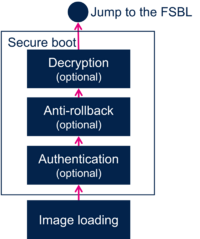
5. Secure boot[edit source]
The ROM code implements the secure process as described in STM32 MPU ROM code secure boot.
If the Secure boot is successful, then the ROM code stores the address of the boot context in r0 register and jumps to the FSBL entry point defined in image header.
5.1. Cryptographic accelerators (ECDSA, AES)[edit source]
On the STM32MP13x lines ![]() and STM32MP2 series, the ROM code uses HASH, PKA, CRYP, and SAES cryptographic accelerators.
and STM32MP2 series, the ROM code uses HASH, PKA, CRYP, and SAES cryptographic accelerators.
- HASH to perform SHA256 hashes.
- PKA to perform ECDSA signature verification
- CRYP or SAES to perform AES decryption of the FSBL. By default CRYP is used. Peripheral usage is defined in the OTP:
- On STM32MP13x lines , OTP CFG9 Bit 7
- On STM32MP25x lines , OTP BOOTROM_CONFIG_7 Bit 8
- On STM32MP13x lines
On STM32MP15x lines ![]() , the ROM code uses HASH cryptographic accelerators, to perform SHA256 hashes.
, the ROM code uses HASH cryptographic accelerators, to perform SHA256 hashes.
6. Secondary core boot[edit source]
6.1. On STM32MP13x lines [edit source]
The device embeds only one Cortex-A7 core.
6.2. On STM32MP15x lines [edit source]
The device embeds two Cortex-A7 cores. At reset, both cores of the Cortex-A7 start and run the same instructions.
The ROM code splits the execution flow so that only core0 runs the boot process. The secondary core of the Cortex-A7 is parked in an infinite loop, waiting for a signal from the application to proceed further. The signal mechanism is based on a secure SGI and the two backup registers
MAGIC_NUMBER and BRANCH_ADDRESS.
To unpark core1, the application running on core0 must:
- write jump address into BRANCH_ADDRESS backup register.
- write 0xCA7FACE1 value into MAGIC_NUMBER backup register.
- generate an SGI interrupt to core1.
6.3. On STM32MP25x lines [edit source]
The device embeds a cluster of two Cortex-A35 cores. At reset, both cores of the Cortex-A35 start and run the same instructions. The ROM code splits the execution flow so that only core0 runs the boot process. The secondary core of the Cortex-A35 is parked in an infinite loop.
Once Aarch64 FSBL-A has been authenticated and decrypted, the ROM code program Cortex-A35 reset vector base address in CA35SS_SYSCFG_VBAR_CR register. Then the ROM code start the Aarch64 FSBL-A execution by generating a warm reset of the Cortex-A35 cluster. Both cores of Cortex-A35 cluster start and run the FSBL-A instructions. It is FSBL-A responsibility to implement "holding pen" mechanism for application.
7. Wake up from low power modes[edit source]
The ROM code manages exit from "wake up from low power modes" resulting in a reset.
7.1. On STM32MP13x lines [edit source]
- Standby exit
The ROM code makes no distinction between Standby exit reset and Power On reset.
- LPLV-Stop2 exit
The ROM code reads an address from BSEC SCRATCH register. This address may be any address except a ROM address. If the address is not in ROM range it jumps to it.
7.2. On STM32MP15x lines [edit source]
In the case of Standby exit reset, the ROM code proceeds as shown on following figure:
In such resets, the Cortex®-M4 is always held on reset, and only the ROM code on Cortex®-A7 runs. The behavior of the ROM code depends on value of bits MCU_BEN, MPU_BEN of RCC_MP_BOOTCR register.
- Cortex®-M4 wake up
If bit MCU_BEN of RCC_MP_BOOTCR register is set to 1, the ROM proceeds to Cortex®-M4 software wake up.
The ROM code wakes up Cortex®-M4 by releasing it from its "hold on reset" state.
- Cortex®-M4 software integrity check
- Before releasing Cortex®-M4 the ROM code can use the backup registers to recover the Cortex®-M4 software integrity check value and compare it to the one computed on RETRAM.
- Note: if the device is closed, this check is mandatory.
- Cortex®-A7 wake up
The Cortex®-A7 software wake up consists in processing Secure boot.
The ROM proceeds to Cortex®-A7 software wake up in three cases:
- If M4 software wake up is not required (that is, MCU_BEN=0)
- If M4 software wake up is required (that is, MCU_BEN=1) but fails,
- If M4 software wake up is required (that is, MCU_BEN=1), is processed successfully and MPU_BEN is also set to 1
- Cortex®-A7 returns to CStandby low power mode
If Cortex®-M4 software wake up is required (that is, MCU_BEN=1), is processed successfully and MPU_BEN is set to 0, the ROM enters the Cortex®-A7 in CStandby low power modes.
7.3. On STM32MP2 series[edit source]
7.3.1. Wake up in CA35 cold boot mode[edit source]
In CA35 cold boot mode, Cortex-A35 is the master of security and is the processor that starts first at wake up. BootROM is the first software to run and detects two possible cases:
- D1 DSTANDBY exit while SYSRAM was in retention
- The content of SYSRAM was preserved.
- D1 DSTANDBY exit while SYSRAM was not in retention
- STANDBY exit
- The content of SYSRAM was lost
7.3.2. Wake up in CM33 cold boot mode[edit source]
In CM33 cold boot mode, Cortex-M33 master is the master of security is the processor that starts first at wake up. CM33 is responsible to restore security settings and may wake up CA35. BootROM will run and detect two possible cases:
- D1 DSTANDBY exit while SYSRAM was in retention
- The content of SYSRAM was preserved.
- D1 DSTANDBY exit while SYSRAM was not in retention
- The content of SYSRAM was lost,
7.3.3. D1 DSTANDBY exit while SYSRAM was in retention[edit source]
- The content of SYSRAM was preserved. BootROM will try to jump at address stored in backup register BKPR11 :
- 1- RTC clock shall be enabled (RTCCFGR.RTCEN=1)
- 2- TAMP RIF region R1 shall be allocated to CID1, and CFEN enabled and contain BKP11R
- TAMP_R1CIDCFGR.CID[3:0]=1 (R1 belongs to CID1=CA35)
- TAMP_R1CIDCFGR.CFEN=1 (compartment filtering activated for CID1)
- TAMP_BKPRIFR1.BKPRWRIF[7:0] >= 12 : TAMP_BKP11R in RIF R1 region
- 3- TAMP_BKP11R shall be RW secure
- TAMP_SECCFGR.BKPRWSEC[7:0] >= 12 : TAMP_BKP11R in RW secure region
- 4- Branch address shall be in SYSRAM range: [0x0E000000, 0x0E03FFFF]
- If any of the check above fails, BootROM proceed a boot from flash to load and boot an FSBL-A image.
7.3.4. D1 DSTANDBY exit while SYSRAM was not in retention[edit source]
- STANDBY exit
- The content of SYSRAM was lost, BootROM will proceeds a boot from flash to load and boot an FSBL-A image.
8. Secure services export[edit source]
8.1. On STM32MP13x lines [edit source]
The ROM code does not export any service for the application.
8.2. On STM32MP15x lines [edit source]
The ROM code exports authentication services to the following stages of the STM32MP15 secure boot, starting with the FSBL.
8.3. On STM32MP2 series[edit source]
The ROM code does not export any service for the application.
9. Memory mapping[edit source]
9.1. On STM32MP13x lines [edit source]

The boot context (see boot_api_context_t structure in plat/st/stm32mp1/include/boot_api.h with STM32MP13 compilation flag) is in the first 512 bytes of SRAM2. It contains information on the boot process (such as the selected boot device), and pointers to the ROM code services (used for secure boot authentication).
9.2. On STM32MP15x lines [edit source]

The boot context (see boot_api_context_t structure in plat/st/stm32mp1/include/boot_api.h with STM32MP15 compilation flag) is in the first 512 bytes of SYSRAM. It contains information on the boot process (such as the selected boot device) and pointers to the ROM code services (used for secure boot authentication).
9.3. On STM32MP2 series[edit source]

The boot context (see boot_api_context_t structure in plat/st/stm32mp2/include/boot_api.h with STM32MP15 compilation flag) is in the first 512 bytes of SYSRAM. It contains information on the boot process (such as the selected boot device) and pointers to the ROM code services (used for secure boot authentication).
10. System and peripheral registers modification after boot sequence[edit source]
10.1. On STM32MP13x lines [edit source]
10.1.1. RCC registers[edit source]
10.1.1.1. All cases except Engineering boot[edit source]
Except when boot pins values are equal to 0b100 (Engineering boot), the following clocks are used:
- PLL1 setting changed from reset values:
- PLL1 clock source is kept as default: HSI (64 MHz)
- DIVM+1 = 5, DIVN+1 = 32
- VCO @819.2 MHz
- PLL1_p @409.6MHz (DIVP+1 = 1)
- Cortex-A7 clocked at 409.6 MHz, using PLL1_p source
- PLL2 setting changed from reset values:
- PLL2 clock source is kept as default: HSI (64 MHz)
- DIVM+1 = 5, DIVN+1 = 35
- VCO @896MHz
- PLL2_p @448MHz (DIVP+1 = 1)
- AXI (aclk), AHB5 (hclk5) and AHB6 (hclk6) clocked at 112 MHz, using PLL2_p source.
- AXIDIV+1 = 4
- APB4 (pclk4) clocked at 56 MHz
- APB4DIV = 1 -> pclk4 = aclk/2
- APB5 (pclk5) clocked at 28 MHz
- APB5DIV = 2 -> pclk5 = aclk/4
10.1.1.2. All cases[edit source]
In all cases, the following clocks are also enabled in RCC
- DDRPHYC pclk4 (DDRPHYCAPBEN = 1), together with DDRPHYC APB reset released (DPHYAPBRST = 0)
- STGEN pclk5 and kernel clock (STGENEN = 1)
- ETZPC pclk5 (TZPCEN = 1)
- SYSCFG pclk3 (SYSCFGEN)
In each boot mode, the relevant GPIOA to GPIOZ clocks are enabled depending on interface needed and OTP settings.
10.1.1.3. Engineering boot[edit source]
When boot pins value are equal to 0b100 (Engineering boot), the following settings are done:
- GPIOA hclk4 (GPIOAEN) clock enabled
- TZEN = 0 (RCC TrustZone security is disabled)
- Secure and non-secure debug opened (BSEC_DENABLE = 0x47F)
10.1.1.4. Serial boot[edit source]
When serial boot (USB/UART) is used:
- GPIOA hclk4 (GPIOAEN) clock enabled
- USBPHYC pclk4 and PLL_USB input clock (USBPHYEN = 1)
- The HSE is enabled in crystal, analog bypass or digital bypass according to OSC_OUT setting (refer to the STM32MP13 Reference manuals). When disable HSE bypass detection is set to 1, ROM considers HSE is in oscillator mode.
- HSEON = 1
- HSEBYP = 0 or 1
- DIGBYP = 0 or 1
- The HSE is enabled only in case of USB/UART boot. ROM waits for HSERDY with a timeout of 20ms.
- USB enumeration not maintained after USB boot, USB detach process done.
When HSE detected value is either 8, 10, 12, 14, 16 or 25 MHz, the bootrom uses PLL4_R as an intermediate PLL to set 24 MHz in USBPHY PLL entry.
10.1.2. STGEN registers[edit source]
- STGENC_CNTCR.HLTDBG and EN =1
- STGENC_CNTFID0 = 64000000 (Bootrom uses HSI 64 MHz for STGEN kernel clock)
10.1.2.1. GPIO[edit source]
Depending on Boot interface, GPIOx_MODER, GPIOx_OSPEEDR, GPIOx_PUPDR and GPIOx_AFRH/AFRL are set according to relevant 'Configuration' described above.
After boot on serial boot (USB/UART) or after engi-boot, or if boot error occurs PA13 is set in GPIO mode, Open-Drain, but in High-Z as ODR13=1 :
| IP | Register | Field | Value at reset (hex) | Value after boot (hex) |
|---|---|---|---|---|
| PA13 GPIO registers modifications | ||||
| GPIOA | GPIO_MODER | MODER13 | 3 | 1 |
| GPIO_OTYPER | OT13 | 0 | 1 | |
| GPIO_OSPEEDR | OSPEEDR13 | 0 | 3 | |
| GPIO_ODR | ODR13 | 0 | 1 | |
10.2. On STM32MP15x lines [edit source]
10.2.1. RCC registers[edit source]
10.2.1.1. All cases except Engineering boot[edit source]
Except when boot pins value are equal to 0b100 (Engineering boot), the following clocks are used:
- PLL1 setting changed from reset values:
- PLL1 clock source is kept as default: HSI (64 MHz)
- DIVM+1 = 5, DIVN+1 = 32
- VCO @819.2 MHz
- PLL1_p @409.6MHz (DIVP+1 = 1)
- Cortex-A7 clocked at 409.6 MHz, using PLL1_p source
- PLL2 setting changed from reset values:
- PLL2 clock source is kept as default: HSI (64 MHz)
- DIVM+1 = 5, DIVN+1 = 35
- VCO @448 MHz
- PLL2_p @448MHz (DIVP+1 = 1)
- AXI (aclk), AHB5 (hclk5) and AHB6 (hclk6) clocked at 149.33 MHz, using PLL2_p source.
- AXIDIV+1 = 3
- APB4 (pclk4) clocked at 74.66 MHz
- APB4DIV = 1 -> pclk4 = aclk/2
- APB5 (pclk5) clocked at 37.33 MHz
- APB5DIV = 2 -> pclk5 = aclk/4
10.2.1.2. All cases[edit source]
In all cases, the following clocks are also enabled in RCC
- DDRPHYC pclk4 (DDRPHYCAPBEN = 1), together with DDRPHYC APB reset released (DPHYAPBRST = 0)
- USBPHYC pclk4 and PLL_USB input clock (USBPHYEN = 1)
- STGEN pclk5 and kernel clock (STGENEN = 1)
- ETZPC pclk5 (TZPCEN = 1)
- RTC/TAMP/BackupReg pclk5 (RTCAPBEN = 1)
- HASH1 hclk5 (HASH1EN = 1)
- SYSCFG pclk3 (SYSCFGEN)
- GPIOA hclk4 (GPIOAEN)
In each boot mode, the relevant GPIOA to GPIOZ clocks are enabled depending on interface needed and OTP settings
10.2.1.3. Engineering boot[edit source]
When boot pins value are equal to 0b100 (Engineering boot), the following settings are done:
- TZEN = 0 (RCC TrustZone security is disabled)
- BOOT_MCU = 1 (MCU is running an infinite loop from RETRAM)
10.2.1.4. Serial boot[edit source]
When serial boot (USB/UART) is used:
- The HSE is enabled in crystal, analog bypass or digital bypass according to OSC_OUT setting (refer to the STM32MP15 Reference manuals). When OTP WORD9.disable_bypass_detection_disable is set to 1, ROM considers HSE is in oscillator mode.
- HSEON = 1
- HSEBYP = 0 or 1
- DIGBYP = 0 or 1
- The HSE is enabled only in case of USB boot. ROM waits for HSERDY with a timeout of 20ms.
- Relevant UART clocks are enabled on HSI
When HSE detected value is either 8, 10, 12, 14, 16 or 25 MHz, the bootrom uses PLL4_R as an intermediate PLL to set 24 MHz in USBPHY PLL entry.
Listened UARTs RX are configured in autobaud, meaning that host has to send 0x7F as very first character and that UART IP will configure itself automatically when receiving this very first character.
10.2.2. STGEN[edit source]
- STGENC_CNTCR.HLTDBG and EN =1
- STGENC_CNTFID0 = 64000000 (Bootrom uses HSI 64 MHz for STGEN kernel clock)
10.2.3. GPIO[edit source]
Depending on Boot interface, GPIOx_MODER, GPIOx_OSPEEDR, GPIOx_PUPDR and GPIOx_AFRH/AFRL are set according to relevant 'Configuration' described above.
After boot on any interfaces (following system reset or standby wake-up) or after engi-boot, PA13 is set in GPIO mode, Open-Drain, but in High-Z as ODR13=1 :
| IP | Register | Field | Value at reset (hex) | Value after boot (hex) |
|---|---|---|---|---|
| PA13 GPIO registers modifications | ||||
| GPIOA | GPIO_MODER | MODER13 | 3 | 1 |
| GPIO_OTYPER | OT13 | 0 | 1 | |
| GPIO_OSPEEDR | OSPEEDR13 | 0 | 3 | |
| GPIO_ODR | ODR13 | 0 | 1 | |
10.3. On STM32MP25x lines [edit source]
will be defined later in STM32MP25 registers modifications after boot sequence article.
11. Debug and error cases[edit source]
11.1. Debug and error messages[edit source]
- Debug GPIO management
- The ROM code uses a dedicated GPIO (assignment depends on STM32MPU device) to communicate some statuses. On STMicroelectronics boards, the GPIO is connected to the red LED, as explained in the LEDs and buttons on STM32 MPU boards article.
- In the case of boot failure, this GPIO pin is set to low open-drain (that is, the red LED lights brightly).
- During UART/USB boot, it toggles open-drain at a rate of about 5 Hz until a connection is started (that is, red the LED blinks fast).
- In STM32MP1 series engineering boot or in STM32MP2 series developper boot, used for specific debug, it toggles opendrain at a rate of about 5 kHz (that is, the red LED light is dim).
- In all other cases, it is kept in it’s reset value, that is, high-Z until software setting.
- On STM32MP1 series, the debug GPIO is PA13 and on STM32MP2 series, it is PH4.
- Traces
- During its execution, the ROM writes binary traces into memory.
- Traces can be downloaded and analyzed with the ROM trace analyzer tool.
- In the case of an internal blocking error, the ROM code writes a UART log error at 9600 bauds to the debug GPIO pin.
11.2. Common debug and error cases[edit source]
- Memory boot failure
- Secure boot flow always enters the serial boot loop during which the Error LED blinks. Therefore, observing such blinking when Memory boot is required indicates that Memory boot failed.
- Security issue
- If the boot ROM encounters a security issue, it stops the secure boot immediately, and sets the Error LED to light brightly.
12. Fuses used by ROM code[edit source]
Arm® is a registered trademark of Arm Limited (or its subsidiaries) in the US and/or elsewhere. ![]()
Arm® is a registered trademark of Arm Limited (or its subsidiaries) in the US and/or elsewhere. ![]()