This article provides an overview of STM32MP257x-EV1 Evaluation boards.
1. Article purpose[edit source]
This article briefly describes:
- How to assemble together the different elements provided in the commercial box
- What are the different components present on the boards
- How to connect the boards to external material
- How to configure the board for boot
- How to select RS232 UART or ST-LINK/V2-1 connectors
- What are the configurations of the connectors pins
This article is valid for the STM32MP257F-EV1 ![]() , Evaluation boards: the part numbers are specified in the STM32MP25 microprocessor part numbers article.
, Evaluation boards: the part numbers are specified in the STM32MP25 microprocessor part numbers article.
2. Board assembly[edit source]
The STM32MP257x-EV1 Evaluation boards packages (STM32MP257F-EV1 ![]() ), completed by the B-CAMS-IMX package, include all the items listed below.
), completed by the B-CAMS-IMX package, include all the items listed below.
")
| Position | Description |
|---|---|
| 1 | MB1936 main board |
| 2 | 7” LVDS WSVGA display with touch panel (EDT ETML0700Z9NDHA panel - optional) |
| 3 | LVDS display cable |
| 4 | MB1854 board AI camera (not part of STM32MP257x-EV1 Evaluation boards packages , provided via B-CAMS-IMX package) |
| 5 | camera board FFC (not part of STM32MP257x-EV1 Evaluation boards packages, provided via B-CAMS-IMX package) - optional |
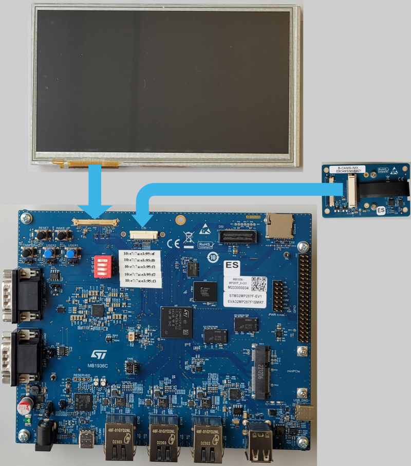
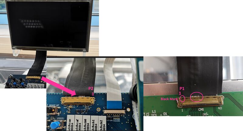
2.1. How to connect LVDS display to MB1936[edit source]
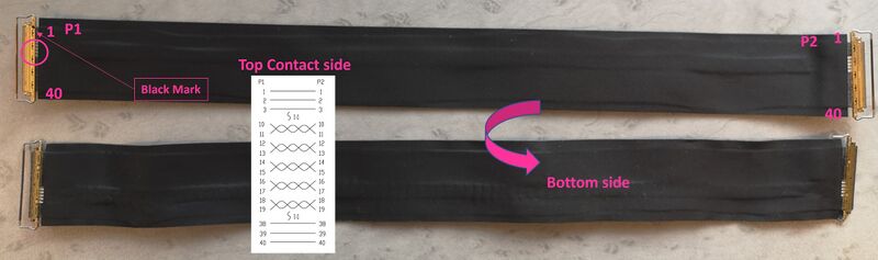
- Check the above cable orientation thanks to the black mark and the white twisted pairs.
- Find the LVDS port on STM32MP257x-EV1 Evaluation board (CN2) and the one on the display (CN1). One cable is provided in the STM32MP257x-EV1 Evaluation board box.
- On each port, insert the cable as described:
2.2. STM32MP257x-EV1 Evaluation board assembled[edit source]

3. Board overview[edit source]
| Position | Description |
|---|---|
| 1 | MB1936 main board |
| 2 | LVDS display |
| 3 | LDVS display connector |
| 4 | MB1854 daughterboard camera (provided via B-CAMS-IMX package) |
| 5 | Camera board connector (provided via B-CAMS-IMX package) |
| Position | Description | Position | Description |
|---|---|---|---|
| 1 (LED1) | User LED (blue) | 2 (LD1) | User LED (red) |
| 3 (LD2) | User LED (orange) | 4 (LD3) | User LED (green) |
| 5 (B1) | RESET button | 6 (B2) | WAKE UP button |
| 7(B3) | TAMPER button | 8 (B4) | USER2 button |
| 9 (B5) | USER1 button | 10 (CN2) | LVDS connector |
| 11(CN4) | CSI connector | 12(CN3) | DSI connector |
| 13 (CN1) | microSD Card connector | 14 (SW1) | Boot mode selection |
| 15 (U22) | S-NOR 512Mb | 16 (CN5) | GPIO Expansion connector |
| 17 (CN9) | FDCAN1 | 18 (CN11) | FDCAN2 |
| 19 (U26) | STPMIC25 | 20 (U27) | STM32MP257 |
| 21 (U24) | eMMC 4GB | 22 (U29) | DDR4 2GB |
| 23(U28) | DDR4 2GB | 24 (CN10) | PWR measurements connector |
| 25 (CN22) | MIPI10 connector | 26 (|CN13) | Mini-PCIe connector |
| 27 (JP4) | Power Jumper | 28 (CN13) | 5V/3A Power Supply Jack |
| 29 (CN21) | USB Power – STLINK TypeC | 30 (CN16) | ETHERNET 2 |
| 31 (CN17) | ETHERNET 1 | 32 (CN18) | ETHERNET 3 |
| 33 (CN19) | Dual USB Host TypeA | 34 (CN15) | USB2.0 DRD TypeC |
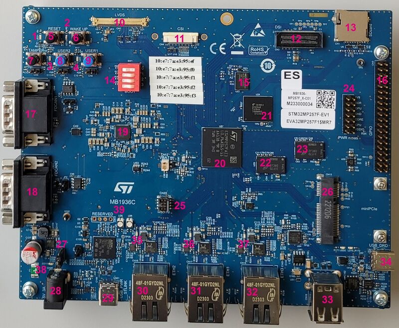
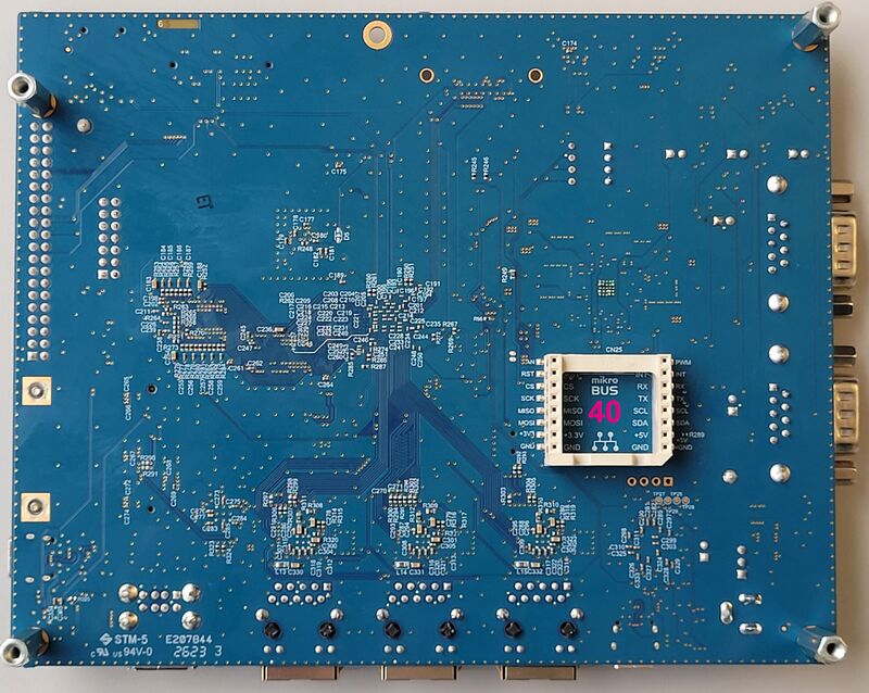
| Position | Description |
|---|---|
| 35(CN35) | mikroBUS connector |
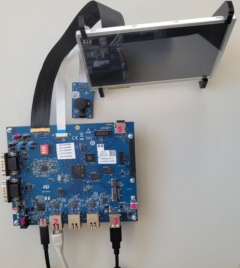
4. Board connection[edit source]
The connections shown in the picture below are the ones recommended to start with the STM32MP257x-EV1 Evaluation boards. As shown in the board overview, other connectors are available for this board (for example CAN).
5. Switches and jumpers[edit source]
Most of default settings of the switches and jumpers shall be kept as set in the commercial box.
There are 2 main exceptions:
- the jumpers related to Power
- the switches related to boot
The sections below detail the main boot switches and the power jumpers.
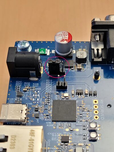
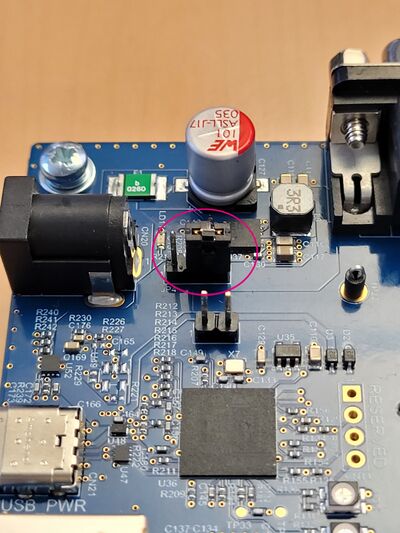
5.1. Power jumper[edit source]
According to the positions presented in the table below, the power jumper (#JP4) allows either the supply the MB1936 board with :
- a 5V/3A power supply unit (not provided with the STM32MP25 EVAL board pack) on the jack #CN20 ,
- a USB Power TypeC #CN21 (USBcable not provided with the STM32MP25 EVAL board pack)
| Jumper | Setting | Configuration |
|---|---|---|
| JP4 | JP[1-2] | Select the USB Power TypeC CN21 as main board supply - USC typeC cable |
| JP4[2-3] | Select the 5V/3A Power Supply Unit on jack CN20 as main board supply |
[edit source]
The STM32MP257x-EV1 Evaluation boards can boot from different Flash devices (microSD, eMMC...); using the microSD card is recommended.
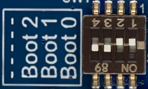
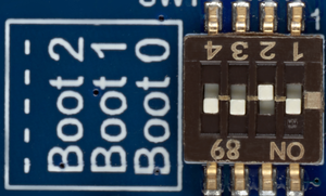
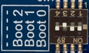
| Boot mode | Boot 2 | Boot 1 | Boot 0 |
|---|---|---|---|
| Engineering boot | 1 | 0 | 0 |
| NOR | 0 | 0 | 1 |
| microSD card | 1 | 0 | 1 |
| eMMC | 0 | 1 | 0 |
| NAND | 0 | 1 | 1 |
| Forced USB boot for flashing |
0 | 0 | 0 |
The boot related switches (SW1 on the board overview picture) must be configured as illustrated by one of the following pictures:
File:STM32MP257x-EV1 boot switches NOR.png Boot from NOR | |
File:STM32MP257x-EV1 boot switches eMMC.png Boot from eMMC | |
File:STM32MP257x-EV1 boot switches forced USB.png Forced USB boot for flashing |
[edit source]
The UART4 is shared exclusively between 2 connectors:
- RS232, D-type, 9-pin connector (CN12 on the board overview picture), dedicated to communication through RS232,
- USB micro-B (ST-LINK/V2-1) (CN4 on the board overview picture), dedicated to the RS232 of ST-LINK/V2-1 controller
The connection is switched by setting JP4 and JP5 jumpers as shown in following pictures:
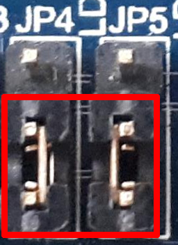 UART4 is connected to the RS232, D-type, 9-pins CN12 connector |
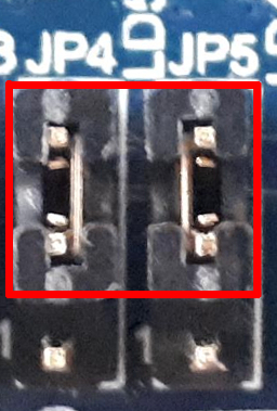 UART4 is connected to the USB micro-B ST-LINK/V2-1 CN4 connector |
6. GPIO mapping[edit source]
6.1. Motor control connector[edit source]
The pins of the motor control connector (CN22 on the board overview picture) are described in the following table.
Due to the sharing of some IOs by multiple peripherals, the motor control interface is not enabled by default, and the motor control cannot be operated simultaneously with the camera, audio codec, CAN and GPIO expansion (GPIO6, 7 and 12): more details (e.g. enabling the motor control interface) in the STM32MP257x-EV1 Evaluation boards user manuals.
| Description | Function | STM32 pin | Pin | Pin | STM32 pin | Function | Description |
|---|---|---|---|---|---|---|---|
| Emergency Stop | TIM8_BKIN | PA6 | 1 | 2 | - | - | GND |
| MC_UH | TIM8_CH1 | PI5 | 3 | 4 | - | - | GND |
| MC_UL | TIM8_CH1N | PH13 | 5 | 6 | - | - | GND |
| MC_VH | TIM8_CH2 | PI6 | 7 | 8 | - | - | GND |
| MC_VL | TIM8_CH2N | PH14 | 9 | 10 | - | - | GND |
| MC_WH | TIM8_CH3 | PI7 | 11 | 12 | - | - | GND |
| MC_WL | TIM8_CH3N | PH15 | 13 | 14 | PA3 | ADC_1_IN15 | Bus Voltage |
| PhaseA current | ADC_1_IN6 | PF12 | 15 | 16 | - | - | GND |
| PhaseB current | ADC_1_IN0 | ANA0 | 17 | 18 | - | - | GND |
| PhaseC current | ADC_2_IN1 | ANA1 | 19 | 20 | - | - | GND |
| NTC ByPass | GPIO | PF3 | 21 | 22 | - | - | GND |
| Dissipative Brake | TIM12_CH1 | PH6 | 23 | 24 | - | - | GND |
| 5V | - | - | 25 | 26 | PF11 | ADC_1_IN2 | Heatsink Temperature |
| PFC Sync | TIM4_ETR | PE0 | 27 | 28 | - | - | 3V3 |
| PFC PWM | TIM4_CH3 | PB8 | 29 | 30 | - | - | GND |
| Encoder A | TIM5_CH1 | PH10 | 31 | 32 | - | - | GND |
| Encoder B | TIM5_CH2 | PH11 | 33 | 34 | PH12 | TIM5_CH3 | Encoder Index |
6.2. GPIO expansion connector[edit source]
The pins of the GPIO expansion connector (CN21 on the board overview picture) are described in the following table:
| Function | STM32 pin | Pin | Pin | STM32 pin | Function |
|---|---|---|---|---|---|
| 3V3 | - | 1 | 2 | - | 5V |
| GPIO2 / I2C5_SDA[EX 1] | PA12 | 3 | 4 | - | 5V |
| GPIO3 / I2C5_SCL[EX 1] | PA11 | 5 | 6 | - | GND |
| GPIO4 / MCO1 | PI11 | 7 | 8 | PB10 | GPIO14 / USART3_TX |
| GND | - | 9 | 10 | PB12 | GPIO15 / USART3_RX |
| GPIO17 / USART3_RTS | PG8 | 11 | 12 | PI5 | GPIO18 / SAI2_SCKA [EX 2] |
| GPIO27 / SDMMC3_D3 | PD7 | 13 | 14 | - | GND |
| GPIO22 / SDMMC3_CK | PG15 | 15 | 16 | PF1 | GPIO23 / SDMMC3_CMD |
| 3V3 | - | 17 | 18 | PF0 | GPIO24 / SDMMC3_D0 |
| GPIO10 / SPI1_MOSI | PZ2 | 19 | 20 | - | GND |
| GPIO9 / SPI1_MISO | PZ1 | 21 | 22 | PF4 | GPIO25 / SDMMC3_D1 |
| GPIO11 / SPI1_SCK | PZ0 | 23 | 24 | PZ3 | GPIO8 / SPI1_NSS |
| GND | - | 25 | 26 | - | GPIO7 / RPI_GPIO7 |
| ID_SD / I2C2_SDA | PH5 | 27 | 28 | PH4 | ID_SC / I2C2_SCL |
| GPIO5 / MCO2 | PG2 | 29 | 30 | - | GND |
| GPIO6 / TIM2_CH4 | PA3 | 31 | 32 | PH6 | GPIO12 / TIM12_CH1 |
| GPIO13 / TIM8_CH4 | PI2 | 33 | 34 | - | GND |
| GPIO19 / SAI2_FSA[EX 2] | PI7 | 35 | 36 | PI10 | GPIO16 / USART3_CTS |
| GPIO26 / SDMMC3_D2 | PF5 | 37 | 38 | PI6 | GPIO20 / SAI2_SDA[EX 2] |
| GND | - | 39 | 40 | PF11 | GPIO21 / SAI2_SDB[EX 2] |
- ↑ 1.0 1.1 The I2C5 is shared between the I2C EXT connector and the GPIO expansion connector. By default, the I2C5 is connected to the I2C EXT connector thanks to Solder Bridges: more details in the STM32MP257x-EV1 Evaluation boards user manuals.
- ↑ 2.0 2.1 2.2 2.3 The SAI2 is shared between the audio codec and the GPIO expansion connector. By default, the SAI2 is connected to the audio codec thanks to Solder Bridges: more details in the STM32MP257x-EV1 Evaluation boards user manuals.
6.3. JTAG connector[edit source]
The pins of the JTAG connector (CN14 on the board overview picture) are described in the following table:
| Function | Pin | Pin | Function |
|---|---|---|---|
| Power | 1 | 2 | Power |
| NJTRST | 3 | 4 | GND |
| JTDI | 5 | 6 | GND |
| JTMS / SWDIO | 7 | 8 | GND |
| JTCK / SWCLK | 9 | 10 | GND |
| Pull down | 11 | 12 | GND |
| JTDO / SWO | 13 | 14 | GND |
| NRST | 15 | 16 | GND |
| Pull down | 17 | 18 | GND |
| pull down | 19 | 20 | GND |
6.4. User buttons and LEDs[edit source]
The GPIO assignments for the user buttons and LEDs are described in the following table. Refer to LEDs and buttons on STM32 MPU boards article to get information on the functional mapping for each one.
| LED color and label | Button label | GPIO |
|---|---|---|
| Green LD3 (*) | USER1 (*) | PA14 |
| Red LD2 (*) | USER2 (*) | PA13 |
| Orange LD4 | - | PD8 |
| Blue LD5 | - | PD9 |
7. References[edit source]