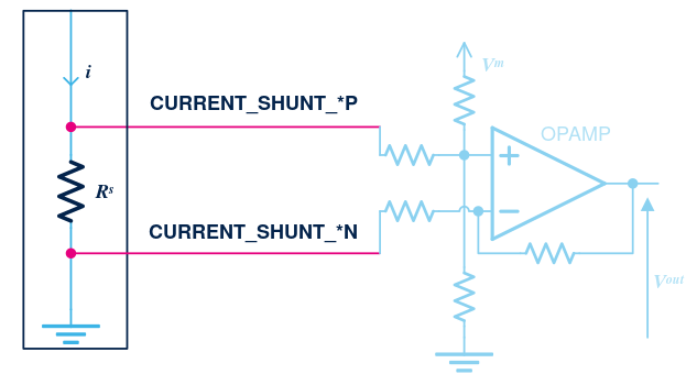
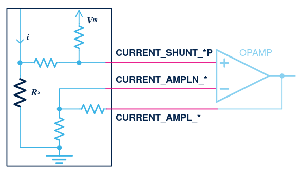
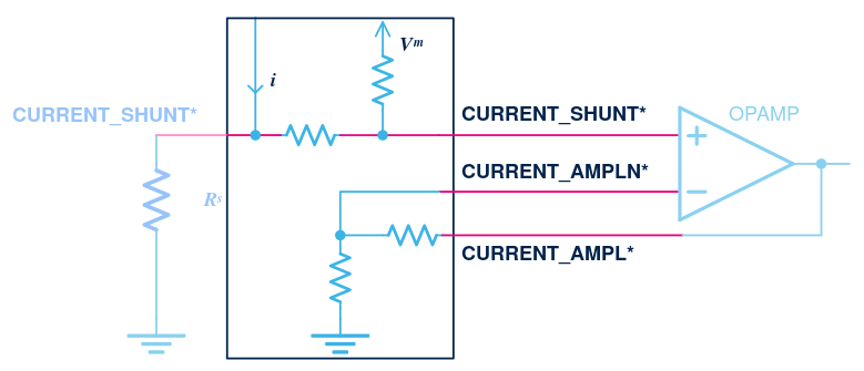
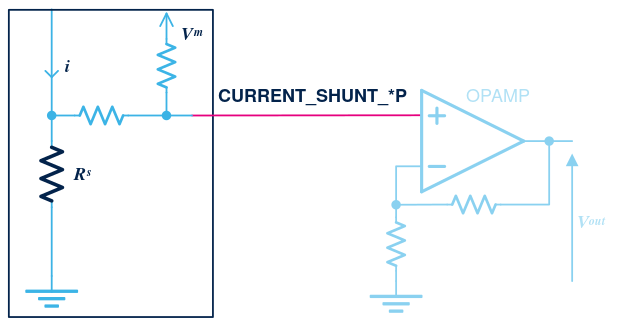
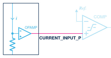
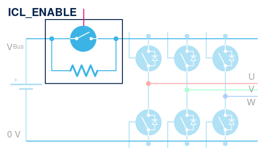
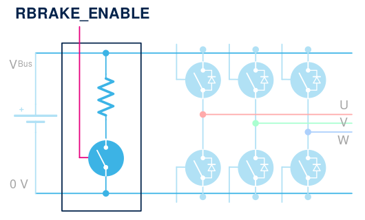
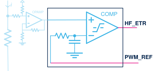
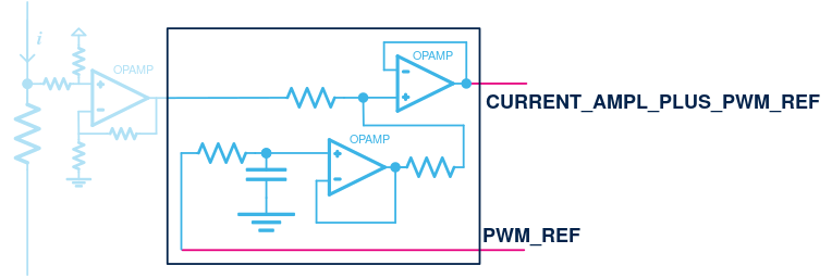
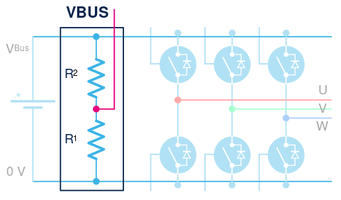
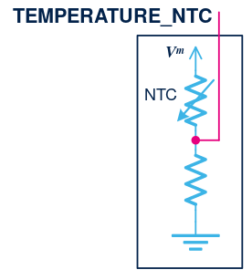
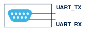
This document specifies the formats used to describe the boards and the other hardware items that are involved in the configuration of a motor-control application. These descriptions are used by the ST motor-control workbench to enable users to configure their motor-control application and produce a software project that implements it following its hardware component features.
1. Board description concepts
1.1. Introduction
From the motor-control workbench perspective, the hardware of a motor-control application is built by combining the following elements:
- An STM32 MCU that executes the software of the motor-control application.
- A control stage that hosts the STM32 device. The control stage embeds all the electronics needed to operate the MCU and may also optionally offer other features that can be of interest in a motor-control application: buttons, potentiometers, or even current sensing circuitry…
- One or more power stages that host all the power electronics needed to drive one or more motors: MOSFETs, drivers, current sensing, and the back-EMF sensing circuitries…
- Motors and their optional speed and position sensors
The ST motor-control workbench must properly connect these elements and configure the MCU according to their characteristics.
These elements are arranged into boards that users plug together to make a motor-control application. Control boards embed an MCU and a control stage. Power boards embed a power stage. Control boards and power boards provide connectors so that they can be connected to one another.
In the ST board portfolio, several incompatible connectors exist. To be able to connect control and power boards despite incompatible connectors, Bridge boards (also called adapters) are provided.
Finally, inverter boards feature an MCU, a control stage, and one or more power stages on a single board.
This document specifies the formats for describing control boards, power boards, inverter boards, and bridges. It may later be extended to cover motors as well.
This document is specifically intended for motor-control SDK users who need to develop the hardware of their motor-control application. In this context, it is expected that such hardware would be described as an inverter.
1.2. General concepts
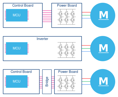
A typical motor-control application is built by plugging a motor into a power board, which is in turn plugged into a control board on which an STM32 MCU is soldered. Alternatively, a motor can be plugged into an inverter board on which an STM32 MCU is soldered. Sometimes, if the connectors available on the control and the power boards differ and are not compatible, an adaptor board (a bridge) is used to connect them. These three motor-control application topologies are depicted in the figure below.
1.2.1. Features
All these boards offer features that can be used by the STM32 MCU.
Some of these features are quite general and can be useful in many different applications, like potentiometers for instance. Others are very specific to a narrow set of applications like Hall-sensors-based current sensing circuitries that specifically target motor control.
Some are very simple and require very little MCU resources like push buttons, for instance, that can be handled by almost any single GPIO of an STM32 device. Others can be a lot more complex and require the use of more advanced MCU functions. A good example of this is the motor-phase voltage generation feature that requires an advanced timer with three of its channels, and six MCU pins (to control both the high and low sides of the phase driving bridge).
But all these features have one key thing in common: they consist of a hardware implementation tied to the pins of the MCU via one or more signals. To be properly used, these signals need to be connected, through these pins, to the peripherals of the STM32 MCU that can handle them.
So, the main purpose of board descriptions is to list the features provided by the boards, describe their characteristics (the signals they offer as interface and the parameters that define them), and how they can find their ways to suitable MCU pins.
1.2.2. Hardware variants
Each feature implemented on a board serves a purpose: A Button is meant for triggering events on the MCU or providing it with a discrete input, and another Potentiometer allows for providing an analog input value to the MCU and the CurrentSensing feature aims at measuring the currents flowing through the phases of a motor, just to give a few examples.
In the board descriptions, features are named and identified after that purpose. However, there are often several different ways of implementing a feature, each with its parameters and set of signals.
A hardware variant is a specific hardware implementation of a feature available on a board. So, describing a feature on a board means describing the hardware variant implemented on that board. For example, the CurrentSensing feature can be implemented by measuring the voltage across shunt resistors. The feature can be implemented with three shunt resistors, one per phase, or with only a single-shunt resistor. These two different hardware implementations are described by different hardware variants that define different signals.
A board can implement several different hardware variants for a given feature. For instance, the X-NUCLEO-IHM16M1 power board implements both a single-shunt and a three-shunt current sensing hardware variant. This is reflected in board descriptions that list all the hardware variants available for the implemented features.
A board that implements several hardware variants of a feature can do so concurrently, independently, or in a combination of both.
Concurrently means that the user has to choose one and only one of the available hardware variants to use the feature. This is what happens with the current sensing on an X-NUCLEO-IHM16M1 power stage: the user chooses between the three-shunt and the single-shunt hardware variants; they cannot use both at the same time.
Independently means that several instances of a feature are provided on the board, each implementing a different hardware variant and they can be all used at the same time. An example would be a control board that would provide several Buttons. Each can be used independently of the others, for different purposes.
The combination of the above exists when a board provides several independent instances of a feature, each implementing several, concurrent hardware variants.
1.2.3. Signals
Signals are the physical interface that features provide (usually) with the MCU. The signals defined by a feature (meaning by a hardware variant of a feature) on a board are meant to be handled by the MCU. They can be an input of the MCU as the voltage across a shunt that can be read by an ADC peripheral or they can be an output of the MCU like a GPIO used to switch a relay, for instance.
Signals have a nature and a name. This nature tells what the signal is used for, and it determines how it must be handled. The name identifies a signal and so its exact role in the feature (and its nature can be deduced).
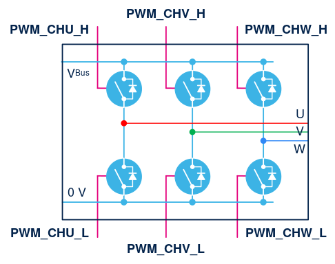
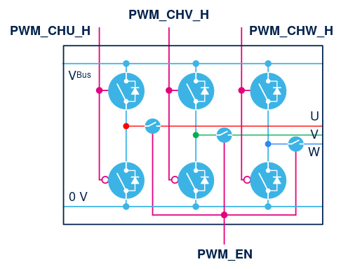
As an example, the figure below shows the DrivingHighAndLowSides hardware variant of the PhaseVoltageGeneration feature. This hardware variant defines six signals: PWM_CHU_H, PWM_CHU_L, PWM_CHV_H, PWM_CHV_L, PWM_CHW_H, and PWM_CHW_L that the MCU drives to control the high- and low-sides switches of the phase driving bridges.
The six signals transport a low-voltage PWM signal that is produced by the PWM output of a timer peripheral that is embedded in the MCU. This is their nature (in this specific case, the six signals have the same nature). The role of PWM_CHU_H is to drive the high-side switch of phase U of a motor. That of PWM_CHV_L is to drive the low-side switch of phase V of the motor. The workbench knows the names of the signals defined by each hardware variant of each feature and uses this knowledge to configure the application properly according to the role and the nature of each of them.
The implementation of this hardware variant also uses other physical signals like bus and 0 Volt supplies (labeled VBus and 0 V in the figure) or the U, V, and W phase lines. However, none of them are plugged into the MCU, so they are not included in the descriptions.
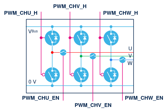
The next figure shows the DrivingHighSidesAndThreeEnables hardware variant of the same feature. Although it defines the same number of signals, the variant differs from the previous one and some of the signals do not have the same nature. They need to be handled differently by the MCU and this is why a different hardware variant is needed. Here, the role of PWM_CHU is to drive phase U of the motor globally leaving the precise driving of the high and low-side switches to the driver, and the role of PWM_CHV_EN is to enable or disable the driving of phase V.
Different hardware variants define different signals or different parameters, but, more importantly, they require different handling from the MCU.
1.2.4. Terminals and pins
Signals must be routed to MCU pins to be used. An important aspect of the description of a signal is to specify how it can be connected to the MCU.
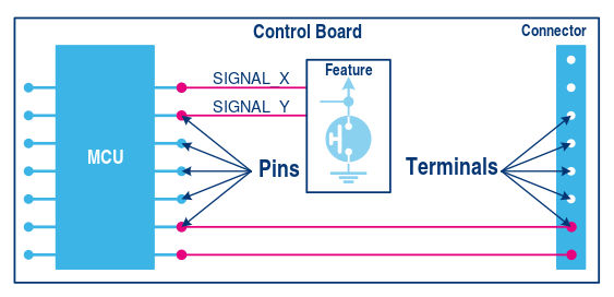
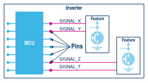
Control boards and inverters host an STM32 MCU. So, the descriptions of the signals provided by the features they implement specify the MCU pins to which they are connected. In this case, the signals are directly linked to the MCU by the description. The following two figures illustrate this.
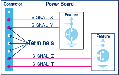
As can be seen above, the terminals of the connector are routed to the pins of the MCU. Most (if not all) of the terminals of the connectors that are soldered on a control board are routed to MCU pins.
Control boards also implement features, and the signals that these features provide are also routed to the pins of the MCU.
A typical inverter does not host a connector since it combines a control stage and one (or more) power stages on the same board. As such, it has an MCU. So, the signals of the features it provides are directly connected to the pins of that MCU.
On the other hand, power boards do not host an STM32. The signals of the features that they implement lead to the terminals of the connector present on these boards. So, the descriptions of signals on these boards specify connector terminals instead of MCU pins. This is depicted in the following figure.
These signals can then be linked to pins of the MCU thanks to the connector that is also present on control boards and the description of the routing between the terminals of this connector and the pins of the MCU.
1.2.5. Connectors and bridges
Control and power boards need to be physically connected to build a motor-control application. To that end, they feature one or more connectors.
Connectors define terminals to which signals and MCU pins are linked across boards. Connectors on control boards link their terminals to MCU pins directly. Connectors on power boards link to signals of the features implemented on these power boards. These links are specified in the descriptions of the boards. When a power board is plugged into a control board, the signals of the features it implements can be routed to the pins of the MCU through the connector used for the plugging.
Different connector topologies are identified by a connector type in the descriptions. Two boards can be plugged together if and only if they are equipped with connectors of the same type. If that is not the case, bridges exist that feature connectors of both types and link them together. Such bridges allow for the boards to be plugged anyway.
Bridges descriptions specify the mapping between the terminals of two connector topologies.
1.2.6. Connection
So, the hardware of a motor-control application is built by combining an MCU, a control stage, and one or more power stages with their connected motors. From the workbench point of view, this amounts to connecting a selection of boards (and motors) that are described as per this specification.
This connection procedure is an important step in the generation of the firmware of a motor control subsystem. It consists of checking if each of the combined features provided by the hardware can be used by the firmware and how.
A feature can be used if at least one of its hardware variants is implemented (and described…) in the hardware and a hardware variant of a feature can be used if all the signals it defines can be properly connected to the MCU. Several conditions are required for a signal to be properly connected to the MCU:
- The signal must be physically connected to a pin of the MCU. This connection can be done directly or through the use of connectors and bridges. The descriptions of the boards provide all the information for assessing this physical connection.
- The pin of the MCU to which the signal is connected must be accessible to a peripheral that can process the signal. For instance, a signal transporting the measure of a current flowing through the phase of a motor needs to be processed by an ADC. The descriptions of the MCU (that are outside the scope of this document) provide the information needed for that.
- The firmware must be able to configure and use the peripheral connected to the signal. For instance, the PWM signals of the phase-voltage-generation feature need to be plugged into specific channels of specific instances of MCU timer peripherals for the firmware to be able to use them, and these requirements of the firmware on signals extend to hardware variants as a whole: to carry on with the phase-voltage-generation feature, all the PWM driving signals need to be routed to the same timer. Signals are not independent… These requirements are known to the workbench and outside of the scope of the descriptions of the board.
The connection of the boards of a motor-control application is complete if all the features needed for it can be connected. Which features need to be connected depends on the choices made for its design. For instance, an application using the FOC drive technique requires at least the PhaseVoltageGeneration, and the CurrentSensing features while an application using the six-step technique only requires the PhaseVoltageGeneration and the SpeedAndPositionSensing features. In addition, the designers may choose to add other features to the application such as the VBusSensing or OverCurrentProtection or the Button features…
1.2.7. Syntax
The low-level syntactic format used in the descriptions is JSON.
Each of the hardware elements specified here (control board, power board, inverter, or bridge) is defined in a single JSON object. The nature of the element being described is stated in a type attribute of this object. The motor-control workbench expects that each hardware element be described in its file, stored in its assets folder, or a specific user folder.
1.2.8. Summary
Describing a board consists of describing the hardware features that it offers and that interface the MCU. Each feature can be implemented in different ways, identified as hardware variants. A board can provide more than one hardware variant for a given feature. Each hardware variant of a feature is defined by a set of parameters and a set of signals. Signals must be routed to pins of the MCU for it to handle them, and a feature is usable in a motor-control application if and only if all the signals of a hardware variant implemented on the board can be routed to suitable peripherals of the MCU.
From the motor-control workbench perspective, a motor-control application is made of boards plugged together through connectors. The workbench must make sure that the features needed for the motor-control application can be properly handled by the firmware, according to their descriptions.
2. Format specifications
2.1. Format version
This document specifies versions 3 and 4 of the motor control boards description format:
- Version 3 is supported from version 6.1.0 of the ST motor control SDK.
- Version 4 is supported from version 6.2.0 of the ST motor control SDK.
Items that are specific to version 4 of the description are explicitly marked as such.
2.2. Common structure
Each hardware element (power board, control board, inverter, and bridge) is described in its file by a single JSON object. A file describing a board contains exactly one JSON object and only this JSON object. Such a JSON object is named a description object.
Here is an example of the minimal structure of a description object:
 {
    "type": "<board type>",
    "descVersion": 4, /* description format version */
    "contentVersion": "1.0" /* version of the board description */
    "name": "<board name>",

    "PN": "<Part Number>",
    "shortDescription": "...",
    "longDescription": "...",
    "link": "<URL>"
    /* ... */
}
A description object must provide the following properties:
- The
typeproperty specifies the type of the hardware element being described. Its value is a string. The specified values are described in the list below; any other value for this field is invalid:"control": the object describes a control board"power": the object describes a power board"inverter": the object describes an inverter board"bridge": the object describes a bridge (aka an adaptor)
- The
descVersionproperty is an integer that specifies the version of the motor control board description format to which the description object conforms. This property is used by the workbench to decode properly the description. See the format version section above for more details. - The
contentVersionproperty specifies the version of the content of a description. Its value shall comply with theN.Mformat whereNandMare two integer numbers, the major and the minor version number respectively. In board descriptions published by ST, a change in the minor version numberMindicates that bugs in the description have been fixed while a change in the major version numberNindicates that additional board features are described (while they were not in earlier versions of the description). The first published version of a board description hascontentVersionset to "1.0". ThecontentVersionproperty deals with the version of the description and not with the version of the board. Each of the different hardware versions of a same board have their own description. ThecontentVersionproperty is available from version 4 of the description format. - The
nameproperty is a string that gives a user-displayable name of the board."PN": A string that specifies the part number of the board being described. This part number might allow for referring to the board in a nonambiguous way, for instance, to order it.
"shortDescription"and"longDescription": A short and a longer text that acts respectively as a title and a description of the board being described meant to be displayed to users."link": A URL pointing to a web page dedicated to the described board.
2.3. Control board
A control board is described in a JSON object that has a type property set to "control".
A control board hosts exactly one STM32 MCU. It can implement features and it provides one or more connectors. Each connector can be used to plug a power board. So, a control board providing two connectors can drive two motors.
Each connector present on a control board is described in a connector object. Connector objects are placed in a connectors array.
Some of the features implemented by a control board are independent of its connectors (they do not rely on signals coming from other boards plugged into them). These are described in a features array that contains one feature object per feature.
Some other features can only be used with a connector of the board. These are described in the connector object that they relate to. See the connector object section below for all the details.
The MCU is referenced by the mcu property.
2.3.1. Specific properties
A control board description object adds the following properties to the common ones:
mcu: A string that references the MCU. This reference is the part number of the STM32 MCU including the package specifier and excluding the temperature specifier (replaced by anx). For instance:STM32G474QETx.clockSource: A string that indicates the source of the clock. It is used by the workbench to generate the code that configures the clock tree of the MCU. The possible values for this string are listed in the following table. Note that this list is indicative and will change in the future.
| Value | Description | supported MCUs |
|---|---|---|
internal_osc
|
The source of the clock is the internal oscillator. | All MCUs |
8_crystal
|
The source of the clock is an 8 MHz crystal. | All MCUs |
24_crystal
|
The source of the clock is a 24 MHz crystal. | STM32G4xx and STM32G0xx |
48_crystal
|
The source of the clock is a 48 MHz crystal. | STM32G4xx |
clockFrequency: An integer set to the frequency of the MCU, expressed in MHz.connectors: An array of connector objects. Each connector object describes an actual connector installed on the board. A control board must provide at least one connector. So, this array must not be empty.features: An array of feature objects. The connector-independent features must be described in this array. A feature is connector-independent if it can be used even though nothing is plugged into any of the connectors of the control board. Each feature object in the array describes one such feature implemented on the board. This array is empty for a control board that does not provide any connector-independent feature.
2.3.2. Example
A skeleton of a control board description is presented below. For the sake of brevity, the common properties are not shown as well as objects specified elsewhere in this document.
 {
    /* ... */
    "mcu": "STM32<reference>x",
    "clockSource": "24_crystal", /* source of MCU clock */
    "clockFrequency": 170, /* MCU frequency */

    "features": [/*...*/],

    "connectors": [/*...*/]
}
2.4. Power board
A power board is described by a JSON object that has a type property set to "power".
A power board implements the power electronics needed to drive one or more motors. It does not host an STM32 MCU and thus needs to be plugged into a control board for the motor control features it implements to be used. So, a power board must provide at least one connector. Note that in the perspective of ST motor-control SDK, a motor-control application has exactly one STM32 MCU that drives all its motors and thus a power board is only connected to one MCU.
On a power board, a connector is considered an entry point for driving a motor. Beyond this entry point, the power board provides its features. This has three consequences for the description format:
- The connector, as outlined for control board descriptions, only represents a subset of the description needs when it comes to dealing with power boards. So, power boards do not describe
connectorsbut rathermotorDrivesthat slightly differs from the notion of a connector object, adding what is missing describing the power stage. See the motor drive object section for full details. - A connector leads to the power electronics designed to drive one motor. A power board can drive as many motors as it provides connectors (and so motor drives).
- All the features of a power board are connector-dependent and so motor drive dependent. Indeed, the features implemented on a power board are connected to the MCU of the control board through the connector of the motor drive. The main purpose behind the description of a motor drive provided in power boards is to group the description of the features provided by the board.
2.4.1. Specific properties
A power board description adds the following property to the common ones:
motorDrives: An array of motor drive objects. Each motor drive object groups the features installed on the board that are accessible through the connector it represents. A control board must provide at least one connector. So, this array must not be empty.
2.4.2. Example
A skeleton of a power board description is presented below. For the sake of brevity, the common properties are not shown as well as objects specified elsewhere.
 {
    /* ... */
    "motorDrives": [/*...*/]
}
2.5. Inverter
An inverter is described by a JSON object that has a type property set to "inverter".
Inverters consist of an MCU, a control stage, and one or more power stages. They can be seen as a control board on which one or more power boards are plugged. As such, the description of an inverter is a mix of control and power board descriptions.
Like a control board, an inverter hosts one STM32 MCU, and this MCU is described the same way as in a control board.
Like a power board, an inverter implements one or more motor drives, each having the features needed to drive one motor, and these motor drives are described the same way as in a power board, in a motorDrives array.
Finally, still like a control board, an inverter can implement features that are connector-independent. In the context of an inverter, such features do not relate to any of the motor drives implemented on the board. These are described in a features array placed at the root of the description object.
2.5.1. Specific properties
So, an inverter board description adds the following properties to the common ones:
mcu: A string that references the MCU. This reference is the part number of the STM32 including the package specifier and excluding the temperature one (replaced by anx). For instance:STM32G474QETx.clockSource: A string that indicates the source of the clock. It is used by the workbench to generate the code that configures the clock tree of the MCU. See the description of this field in the control board section for a list of its possible values.clockFrequency: An integer set to the frequency of the MCU, expressed in MHz.motorDrives: An array of motor drive objects. Each motor drive object groups the features installed on the board that are accessible through the connector it represents. An inverter must provide at least one motor drive. So, this array must not be empty.features: An array of feature objects. Connector-independent features must be described in this array. A feature is connector-independent if it can be used even though nothing is plugged into any of the connectors of the inverter. Each feature object in the array describes one such feature implemented on the board. This array is empty for an inverter that does not provide any connector-independent feature.
A skeleton of an inverter description is presented below. For the sake of brevity, the common properties are not shown as well as objects specified elsewhere.
 {
    /* ... */
    "mcu": "STM32<reference>x",
    "clockSource": "24_crystal", /* source of MCU clock */
    "clockFrequency": 170, /* MCU frequency */

    "features": [/*...*/],

    "motorDrives": [/*...*/]
}
2.6. Bridge
A Bridge is described by a JSON object that has a type property set to "bridge".
A bridge is an adapter between two types of connectors. Its purpose is to allow for connecting a control and a power board equipped with different connectors.
Bridges have a direction: they have a power board side and a control board side that cannot be exchanged. Both sides provide connectors: power-side connectors on the power board side and control-side connectors on the control board side. A power-side connector of a bridge must not be connected to a control board and a control-side connector must not be connected to a power board. Bridges may feature several power-side connectors that can each lead to several control-side connectors.
Describing a Bridge consists of describing all the power-side connectors that it implements. The description of a power-side connector mainly consists of listing and describing the control-side connectors that it leads to. Finally, each control-side connector describes the associations between its terminals and that of the related power connector.
A Bridge description object adds the following property to the common ones:
powerSideConnectors: An array of power side connector objects. Each element in this array describes a connector provided by the bridge and meant to be plugged into a power board. A bridge provides at least one such connector, so this array cannot be empty.
2.6.1. Power-side connector object
A power-side connector object describes one connector meant to be plugged into a power board. It provides the following properties:
type: A string that identifies the type of the connector being described. See section connectors for a list of the possible values.name: A string that names and identifies the instance of the connector on the bridge. This name can be displayed to workbench users and allows for avoiding confusion between connectors on the board. For instance, the description of a bridge that would feature two connectors of typeMotorControlConnectorwould assign them different names so that users can distinguish them. The value of thenameidentifies a physical connector present on the bridge.controlSideConnectors: An array of control side connector objects. Each element of this array describes a control-side connector, which terminals can be relayed to terminals of the power-side-connector object. The purpose of a bridge is to bind power-side and control-side connectors, so this array cannot be empty.
As a motor-control application is built around exactly one STM32 MCU, a power board can only be connected to one control board. So, only one control-side connector object or a bridge can be used in a motor-control application. The controlSideConnectors array presents a set of alternatives from which at most one is to be chosen for a given application.
2.6.2. Control-side-connector object
A control-side-connector object describes one connector meant to be plugged into a control board. It provides the following properties:
type: A string that identifies the type of the connector being described. See section connectors for a list of the possible values.name: A string that names and identifies the instance of the connector on the bridge. This name can be displayed to workbench users and allows for avoiding confusion between connectors on the board. For instance, the description of a bridge that would feature two connectors of typeMotorControlConnectorwould assign them different names so that users can distinguish them. The value of thenameidentifies a physical connector present on the bridge.powerTerminals: An object describing the mapping between the terminals of the connector described by the control-side-connector object and the terminals of the connector described by the power-side-connector object to which it belongs. Properties of thepowerTerminalsobject are named after the terminals of the power-side connector. Each describes the mapping of the terminal that it is named after. These properties are arrays of pin and terminal objects that list the terminals of the control-side connector onto which the power-side connector terminals they are named after are mapped. Only power-side connector terminals that are mapped onto control-side connector terminals need to be described. Properties of thepowerTerminalsobject that are named after a nonmapped terminal are implicitly set to an empty array, so there is no need to set explicitly them in the description.
A skeleton of a bridge description is presented below. For the sake of brevity, the common properties are not shown as well as objects specified elsewhere.
 {
    /* ... */
    "powerSideConnectors": [
        {
            "name": "<user displayed unique power connector name>",
            "type": "<connector type>",

            "controlSideConnectors": [
                {
                    "name": "<user displayed unique control connector name>",
                    "type": "<connector type>",
                    "powerTerminals": {
                        "<Power Terminal n>": [/* ... */],
                        /* ... */
                    }
                },
                /* ... */
            ]
        },
        /* ... */
    ]
}
2.7. Connector object
A connector object describes the routing between the terminals of a connector installed on a control board and the pins of the MCU hosted on this board. For each terminal, this routing can be direct, or it can go through the electronics of connector-dependent features implemented on the board. In both cases, the routing of terminals is described in a terminals object that describes their connection to MCU pins. If the control board implements features that depend on a connector (see the control board section), these are described in the features property of the related connector object.
A control board can provide more than one connector of any type.
A connector object provides the following properties:
type: A string that identifies the type of the connector being described. See section connectors for a list of the possible values.name: A string that names and identifies the instance of the connector on the control board. This name can be displayed to workbench users and allows for avoiding confusion between connectors on the board. For instance, the description of a control board that would feature two connectors of typeMotorControlConnectorwould assign them different names so that users can distinguish them. The value of thenameidentifies a physical connector present on the bridge.terminals: An object describing the mapping between the terminals of the connector described by the connector object and the pins of the MCU. The properties of theterminalsobject are named after the terminals of the connector. Each consists of an array of pin and terminal objects that lists the pins of the MCU to which the terminal it is named after is connected. Only terminals that are connected to the MCU need to be described. For each terminal that is not connected to the MCU, an implicit property named after it exists and is set to an empty array, so there is no need to define it explicitly.features: An array of feature objects. Features depending on the connector must be described in this array. A feature depends on the connector if it relies on signals connected through the connector to be used. In other words, a feature depends on the connector if it cannot be used when nothing is plugged into the connector. Each feature object in the array describes one such feature implemented on the board. This array is empty and does not need to be defined explicitly if no such feature exists for the connector. In such a case, thefeaturesarray is defined implicitly and set to an empty array.
A connector object always describes one full physical connector.
2.8. Motor drive object
A motor drive object describes the connection between the features implemented on a board to drive one motor and either a connector or an MCU. It is used in power board and inverter descriptions. A motor drive object then describes one power stage. Additionally, a motor drive object can also be used to describe the connections between the terminals of a connector and the pins of the MCU of an inverter.
In power board descriptions, a motor drive object provides the parameters that define its operating range and a description of the features implemented on the board with the connection of their signals to the terminals of the connector.
A motor drive object in an inverter board description does the same thing except that the signals of the features it describes are connected to the pins of the MCU. Inverter boards may also optionally provide connectors to plug external power boards in addition to the power stages they embed. Such connectors are handled with motor drive objects that describe the routing between the terminals of the connectors to the pins of the MCU.
The structure of a motor drive object is very similar to that of a connector object. It defines the following properties:
name: A string that names and identifies the instance of the motor drive on the board. This name can be displayed to workbench users and must be chosen to allow an easy and unambiguous identification of the motor drive on the board.
connectorType: A string that identifies the type of the connector leading to the power stage being described. See section connectors for a list of the possible values. In the case where the motor drive object does not lead to a connector (which is common for an inverter), this property must be set to an empty string. If this property is not set in a description, it is implicitly defined as an empty string.terminals: If theconnectorTypeproperty is not an empty string, this property is set to an object describing the connections between the terminals of the connector described by the motor drive object and the pins of the MCU. The properties of theterminalsobject are named after the terminals of the connector. Each consists of an array of pin and terminal objects that lists the pins of the MCU to which the terminal it is named after is connected. Only terminals that are connected to the MCU need to be described. For each terminal that is not connected to the MCU, an implicit property named after it exists and is set to an empty array, so there is no need to define it explicitly. If theconnectorTypeproperty is not defined or is set to an empty string, theterminalsproperty is set to an empty object. If this property is not set in a description, it is implicitly defined as an empty string.features: An array of feature objects. Features implemented in the power stage must be described in this array. This array is empty and does not need to be defined explicitly if no feature is to be described. This can be the case if theconnectorTypeis not empty and no connector-dependent feature is implemented for the connector referenced by the motor drive object. In such a case, thefeaturesarray is defined implicitly and set to an empty array.
Starting from version 4 of the description format, a motor drive object can also define the following property that enables the ST motor profiler tool for this drive. This property is optional, but it needs to be defined for the motor profiler to work with the board:
resistorOffset: Resistance added by the electronics of the board to that of the motor at the measurement point. The value of theresistorOffsetis subtracted from the raw motor resistance measurement made by the profiler. Then, the actual motor resistance is obtained with the following formula:
Rs = (Rmeasure - offsetResistor)/2
Where Rs is the phase resistance of the motor and Rmeasure the raw measurement made by the profiler firmware.
2.9. Feature object
A feature object advertises the presence of a feature on a board and groups the descriptions of hardware variants of this feature that the board implements. The type of the feature described by a feature object is set in the type property of the object. All the hardware variants whose descriptions are grouped within a feature object must describe implementations of that feature.
A feature object describes one instance of a feature on a board. There can be several instances of a given feature on the same board that can be used simultaneously. Each is then described in its feature object. A good example of this is the button feature. Many ST evaluation boards feature several buttons and each needs to be described to be used,
On another side, an instance of a Feature may provide several, alternative, hardware implementations. In this configuration, only one of them can be used in a given application. These are described as hardware variants in the hwVariants array of the feature object. An example is the current-sensing feature of the X-NUCLEO-IHM07M1 board that provides both a three-shunt and a one-shunt implementation that share the same circuitry. Only one of them can be used at any given time and the choice is made by the user thanks to dedicated jumpers on the board.
A feature object provides the following properties:
type: A string that identifies the type of the feature described by the feature object. This string is normative and known to the workbench. It uniquely identifies the nature of the feature. Known features are specified in the features specification section along with the string that identifies their type.name: Name of the feature described by the feature object. This uniquely identifies the instance of the feature described on the board where the object is defined. If several instances of a feature can coexist in a given board (or in a motor-control application), then several instances, with the same type but different names can be described in a board. Some features are mandatory to build a motor-control application, some are not. This is known to the workbench, which deduces it from the choices of the users.hwVariants: An array of hardware variant objects. Each element of the array describes a hardware variant of the feature supported by the board. The hardware variant of a feature is an actual implementation of that feature. So, if a feature is implemented, there must be at least one hardware feature described and so, this array cannot be empty. The hardware variants described in this array represent alternative implementations of the feature, from which one and only one is to be chosen for the feature to be used. Hardware variants are identified by their type. In the current version of this specification, there must not be two hardware variants of the same type in this array.
The properties defined here are common to all the features. Specific features may add other properties to provide parameters that are specific to their nature.
2.9.1. Hardware variant object
A hardware variant object describes the parameters and the signals that define a hardware variant of a feature. Which signals and parameters to be described are defined for each hardware variant. See the features specification section for a complete description of all known hardware variants.
A hardware variant object provides the following common properties that are defined for all hardware variant object types:
type: A string that identifies the type of the hardware variant described by the hardware variant object. This string is normative and known to the workbench. It uniquely identifies the nature of the hardware variant. Known hardware variants are specified in the features specification section along with the string that identifies their type.help: A short text string that explains what to do to activate the variant of this feature. This string is meant to be displayed to users so that they know what conditions (and possibly modifications) need to be done to their board for the hardware variant to be used.signals: An object describing all the signals defined by the hardware variant. This object defines one property for each signal; the name of the property is the name of the signal. Each of these properties is an array of pin and terminal objects that lists the pins of the MCU or the terminals of a connector to which the signal is connected. Whether the pins and terminal objects describe MCU pins or connector terminals depends on the context in which the enclosing feature object is defined.
A skeleton of a feature description is presented below.
 {
    "name": "<user displayed unique name of the feature>",
    "type": "<feature type>",

    "hwVariants": [
        {
            "type": "<hardware variant type>",
            "help": "...",

            "signals": {
                "signal X": [/* ... */]
            }
        }
    ]
}
2.10. Pin and terminal object
A pin-and-terminal object specifies either an MCU pin or a terminal of a connector with all the information needed to connect it properly. It provides the following properties:
name: A string that names the MCU pin or the connector terminal. MCU pins are named as per the MCU reference manual. Terminals of a connector are named according to the nomenclature defined in the connectors section below.cost: A positive integer, ranging from 0 to 10, that measures how “difficult” it is to use the pin or the terminal represented by the object. It is 0 if there is nothing to do to use the pin for this signal; it is nonzero if there is a modification to make on the board for the pin/terminal to be used. This can be a jumper to move, solder bridges to close or open, a 0-Ohm resistor to solder or unsolder… Most of the time, this property must be set to 0.help: A short text that states what to do to use the pin/terminal.
In all the description formats specified in this document, pin and terminal objects are used in arrays. If a pin and terminal objects array contains more than one element, then either all these elements are connected at the same time, or each element represents an alternative connection or a mix of both. Pins and terminal objects with a zero cost are connected by default.
3. Features specification
Feature names are normative and known to the workbench. Each feature specified here is described in its object type that inherits all the properties of the feature object defined in the feature object section. For each feature, at least one hardware variant is specified. As for the features, hardware variants are described with their object type that inherits all the properties of the hardware variant object.
Each feature object can define its parameters and list of hardware variants. Each hardware variant can define its parameters and provide its signals.
Most of the hardware variant descriptions are illustrated by figures. Each figure depicts a hardware variant in a dark blue box, showing its signals and sometimes placing it in its environment. The schematics displayed in the dark blue boxes are provided as a hint of the nature of the hardware variant only and not as an accurate implementation of it.
3.1. Motor-phase-current-sensing
This feature aims at measuring the currents flowing through the phases of a motor.
The type of this feature is CurrentSensing.
This feature defines the following property:
tRise: An integer. Set to the TRise parameter of the switches used for driving the phases of the motor. The value oftRiseis expressed in nanoseconds.
See current sensing signals conditioning model about shunt signals amplification.
3.1.1. Three-shunt current sensing
Current sensing feature hardware variants using a three-shunt current sensing topology.
3.1.1.1. Three-shunt, amplified current hardware variant
This hardware variant is available on power boards and inverter boards.
The type of this hardware variant is ThreeShunt_AmplifiedCurrents
3.1.1.1.1. Description
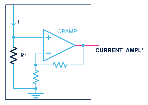
Three shunt resistors are used to measure phase currents (one per phase) and the inverter (or the power board) amplifies the voltages measured across the shunts. The signals coming out of the power stage are connected to ADC peripherals on the MCU. The ADCs are in single-ended mode and the three signals carry the potential on the high side of each shunt resistor, which is then compared to the ground of the MCU. Hence, only three signals are coming out of the power stage for this variant of the feature.
3.1.1.1.2. Properties
| Parameters | Type | Description |
|---|---|---|
tNoise
|
Number | TNoise parameter of the phase switches. In ns |
shuntResistor
|
Number | Shunt resistor value in Ohm |
offsetNetworkAttenuation
|
Number | Gain of the offset network |
opAmpGain
|
Number | Gain of the op amp amplification |
polarizationOffset
|
Number | Shift voltage added by the offset network, in Volts, at op amp output. |
amplifyingNetworkImax
|
Number | Maximum current that is measurable by the current sensing network. |
amplifyingNetworkVm
|
Number | Voltage reference of the current sensing network |
amplifyingNetworkPrating
|
Number | Rated power (that can go through the shunt resistor) |
See current sensing signals conditioning model for complete information on the offsetNetworkAttenuation, opAmpGain, and polarizationOffset properties.
3.1.1.1.3. Signals
| Signals | Description |
|---|---|
CURRENT_AMPL_U
|
Phase U amplified shunt voltage |
CURRENT_AMPL_V
|
Phase V amplified shunt voltage. |
CURRENT_AMPL_W
|
Phase W amplified shunt voltage |
3.1.1.2. Three-Shunt, raw currents, single ended op amp hardware variant
The type of this hardware variant is ThreeShunt_RawCurrents_SingleEnded
This hardware variant is available on power boards.
3.1.1.2.1. Description
Three shunt resistors are used to measure phase currents (one per phase). The power board does not amplify the voltages measured across the shunts or does it offset them. The signals coming out of the power board must then be connected to op amp peripherals on the MCU and to an offset network implemented on the control board. The op amps are in single-ended mode and the three signals carry the potential on the high side of each shunt resistor, which is then compared to the ground of the MCU. Hence, only three signals are coming out of the power stage for this variant of the feature.
This hardware variant can only be found on a power board.
3.1.1.2.2. Properties
| Parameters | Type | Description |
|---|---|---|
shuntResistor
|
Number | Shunt resistor value in Ohm |
3.1.1.2.3. Signals
| Signals | Description |
|---|---|
CURRENT_SHUNT_UP
|
Phase U raw shunt voltage |
CURRENT_SHUNT_VP
|
Phase V raw shunt voltage |
CURRENT_SHUNT_WP
|
Phase W raw shunt voltage |
3.1.1.3. Three-shunt, raw currents, differential op amp hardware variant
The type of this hardware variant is ThreeShunt_RawCurrents_Differential
This hardware variant is available on power boards.
3.1.1.3.1. Description
Three shunt resistors are used to measure phase currents (one per phase). The power board does not amplify the voltages measured across the shunts or does it offset them. The signals coming out of the power board must then be connected to op amp peripherals on the MCU and to an offset network implemented on the control board. The op amps are in differential mode and thus need two signals for each phase to measure the potential difference across each shunt. Hence, six signals are coming out of the power board for this variant of the feature.
This hardware variant can only be found on a power board.
3.1.1.3.2. Properties
| Parameters | Type | Description |
|---|---|---|
shuntResistor
|
Number | Shunt resistor value in Ohm |
3.1.1.3.3. Signals
| Signals | Description |
|---|---|
CURRENT_SHUNT_UP
|
Phase U raw shunt high-side potential to be fed into the noninverting input of an op amp |
CURRENT_SHUNT_VP
|
Phase V raw shunt high-side potential to be fed into the noninverting input of an op amp |
CURRENT_SHUNT_WP
|
Phase W raw shunt high-side potential to be fed into the noninverting input of an op amp |
CURRENT_SHUNT_UN
|
Phase U raw shunt low-side potential to be fed into the inverting input of an op amp |
CURRENT_SHUNT_VN
|
Phase V raw shunt low-side potential to be fed into the inverting input of an op amp |
CURRENT_SHUNT_WN
|
Phase W raw shunt low-side potential to be fed into the inverting input of an op amp |
3.1.1.4. Three-shunt, raw currents, single ended internal op amp with external gain hardware variant
The type of this hardware variant is ThreeShunt_RawCurrents_SingleEnded_ExternalGain.
This hardware variant is available on control boards and inverter boards.
3.1.1.4.1. Description
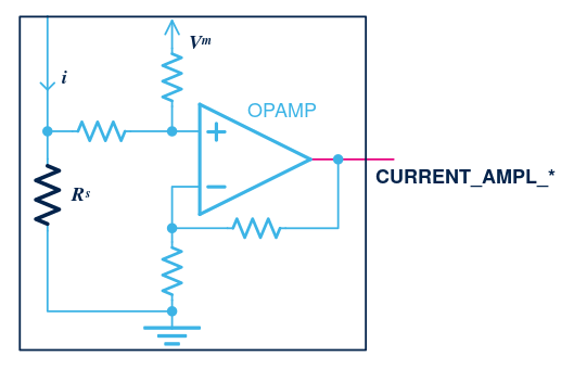
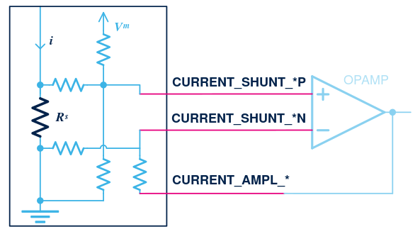
Three shunt resistors are used to measure phase currents (one per phase). The circuitry on the inverter does not amplify the voltages measured across the shunts but it offsets them by a positive shift voltage. The variant provides nine signals among which CURRENT_SHUNT_UP, CURRENT_SHUNT_VP, and CURRENT_SHUNT_WP, that carry the potential on the high side of each shunt resistor offset by the shift voltage. These three first signals are used to compute the values of the currents flowing through the phases of the motor. The six other signals connect the amplifying op amps to the amplification gain circuitry provided by the hardware variant.
The signals coming out of the hardware variant are meant to be connected to op amp peripherals embedded in the MCU. The op amps are configured in single-ended mode and their gain is built outside of the MCU, in the hardware variant. The op amps noninverting inputs are connected to the three shifted current signals CURRENT_SHUNT_UP, CURRENT_SHUNT_VP, and CURRENT_SHUNT_WP. Their inverting inputs are connected to the CURRENT_AMPLN_U, CURRENT_AMPLN_V and CURRENT_AMPLN_W signals; their outputs are connected to the CURRENT_AMPL_U, CURRENT_AMPL_V and CURRENT_AMPL_W signals.
This hardware variant cannot be found on a power board. The following figure provides an overview of it.
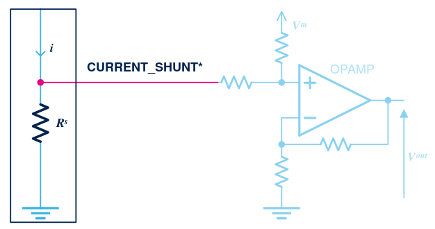
This hardware variant can be used on a control board. In that case, the shunt resistor is not implemented on the control board but rather on the power board that must then implement the three-shunt, raw currents, single ended op amp hardware variant. The complete implementation of the current sensing feature is spread across the control and the power board. Current sensing signals that are coming from the power stage must be connected to the same MCU pin as the ones listed in the control board with the same name. The following figure depicts this flavor of the hardware variant.
The connection of the CURRENT_SHUNT_UP, CURRENT_SHUNT_VP, and CURRENT_SHUNT_WP signals coming from the power board to the proper MCU pins is stated in the terminals object of the connector object in which the hardware variant is described.
3.1.1.4.2. Properties
| Parameters | Type | Description |
|---|---|---|
shuntResistor
|
Number | Shunt resistor value in Ohm. This parameter is optional. Its presence is mandatory for an inverter board. Its value is ignored for a control board. |
offsetNetworkAttenuation
|
Number | Gain of the offset network (the circuitry, in front of the op amps, that adds a positive offset to the voltage measured across the shunt resistor). |
opAmpGain
|
Number | Gain of the op amp amplification |
polarizationOffset
|
Number | Offset of the offset network, in Volts |
amplifyingNetworkImax
|
Number | Maximum current that is measurable by the current sensing network, in Amperes. |
amplifyingNetworkVm
|
Number | Voltage reference of the current sensing network, in Volts |
amplifyingNetworkPrating
|
Number | Rated power (that can go through the shunt resistor), in Watts. |
See current sensing signals conditioning model for complete information on the offsetNetworkAttenuation, opAmpGain, and polarizationOffset properties.
3.1.1.4.3. Signals
| Signals | Description |
|---|---|
CURRENT_SHUNT_UP
|
Phase U raw shunt voltage |
CURRENT_SHUNT_VP
|
Phase V raw shunt voltage |
CURRENT_SHUNT_WP
|
Phase W raw shunt voltage |
CURRENT_AMPL_U
|
Phase U amplified shunt voltage (op amp output) |
CURRENT_AMPL_V
|
Phase V amplified shunt voltage (op amp output) |
CURRENT_AMPL_W
|
Phase W amplified shunt voltage (op amp output) |
CURRENT_AMPLN_U
|
Phase U op amp inverting input. |
CURRENT_AMPLN_V
|
Phase V op amp inverting input. |
CURRENT_AMPLN_W
|
Phase W op amp inverting input. |
3.1.1.5. Three-shunt, raw currents, single ended internal op amp with internal gain hardware variant
The type of this hardware variant is ThreeShunt_RawCurrents_SingleEnded_InternalGain.
This hardware variant is available on control boards and inverter boards.
3.1.1.5.1. Description
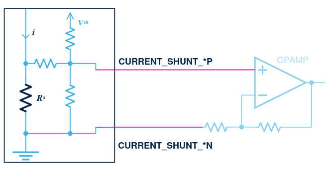
Three shunt resistors are used to measure phase currents (one per phase). The circuitry on the inverter does not amplify the voltages measured across the shunts but it offsets them by a positive shift voltage. The variant provides three signals — CURRENT_SHUNT_UP, CURRENT_SHUNT_VP, and CURRENT_SHUNT_WP — that carry the potential on the high side of each shunt resistor offset by the shift voltage. These signals are used to compute the values of the currents flowing through the phases of the motor.
The signals coming out of the hardware variant are meant to be connected to op amp peripherals embedded in the MCU. These op amps are configured in single-ended mode and the amplification gain is made in the MCU using the PGA. op amps noninverting inputs are connected to the three CURRENT_SHUNT_UP, CURRENT_SHUNT_VP and CURRENT_SHUNT_WP signals. The voltages measured between the potential carried by these signals and the ground of the MCU are amplified by the op amps and then fed into ADCs embedded in the MCU.
This hardware variant cannot be found on a power board. The following figure sketches an overview of it
This hardware variant can also be used on a control board. In that case, the shunt resistor is not implemented on the control board but rather on the power board that must then implement the three-shunt, raw currents, single ended op amp hardware variant. The complete implementation of the current sensing feature is spread across the control and the power board. Current sensing signals that are coming from the power stage must be connected to the same MCU pin as the ones listed in the control board with the same name. The following figure depicts this flavor of the hardware variant.
The connection of the CURRENT_SHUNT_UP, CURRENT_SHUNT_VP, and CURRENT_SHUNT_WP signals coming from the power board to the proper MCU pins is stated in the terminals object of the connector object in which the hardware variant is described.
3.1.1.5.2. Properties
| Parameters | Type | Description |
|---|---|---|
shuntResistor
|
Number | Shunt resistor value in Ohm. This parameter is optional. Its presence is mandatory for an inverter or a power board. Its value is ignored for a control board. |
offsetNetworkAttenuation
|
Number | Gain of the offset network |
opAmpGain
|
Number | Gain of the op amp |
polarizationOffset
|
Number | Shift voltage added by the offset network, in Volts, at op amp output. |
amplifyingNetworkImax
|
Number | Maximum current that is measurable by the current sensing network, in Amperes. |
amplifyingNetworkVm
|
Number | Voltage reference of the current sensing network, in Volts |
amplifyingNetworkPrating
|
Number | Rated power (that can go through the shunt resistor), in Watts. |
See current sensing signals conditioning model for complete information on the offsetNetworkAttenuation, opAmpGain, and polarizationOffset properties.
3.1.1.5.3. Signals
| Signals | Description |
|---|---|
CURRENT_SHUNT_UP
|
Phase U raw shunt voltage |
CURRENT_SHUNT_VP
|
Phase V raw shunt voltage |
CURRENT_SHUNT_WP
|
Phase W raw shunt voltage |
3.1.1.6. Three-shunt, raw currents, differential internal op amp with external gain hardware variant
The type of this hardware variant is ThreeShunt_RawCurrents_Differential_ExternalGain
This hardware variant is available on control boards and inverter boards.
3.1.1.6.1. Description
Three shunt resistors are used to measure phase currents (one per phase). The circuitry on the inverter does not amplify the voltages measured across the shunts. It only provides the offset network. The six current signals (that carry the potential on the high- and low-sides of each shunt resistor) must be connected to the op amp peripherals on the MCU. The op amps are in differential mode and three signals carry the potential on the high side of each shunt resistor to the noninverting inputs while three others carry that of the low sides to the inverting inputs. The inverter provides the current signal offset circuitry and external resistors to make the op amp gain. So, MCU pins are used for op amp noninverting and inverting inputs and op amp outputs.
This hardware variant can be used on a control board. In that case, the shunt resistor is not implemented on the control board but rather on the power board that must then implement the Three-shunt, raw currents, differential op amp hardware variant. The complete implementation of the current sensing feature is spread across the control and the power board. Current sensing signals that are coming from the power stage must be connected to the same MCU pin as the ones listed in the control board with the same name.
3.1.1.6.2. Properties
| Parameters | Type | Description |
|---|---|---|
shuntResistor
|
Number | Shunt resistor value in Ohm. This parameter is optional. Its presence is mandatory for an inverter board. Its value is ignored for a control board. |
offsetNetworkAttenuation
|
Number | Gain of the offset network |
opAmpGain
|
Number | Gain of the op amp amplification |
polarizationOffset
|
Number | Shift voltage added by the offset network, in Volts, at op amp output. |
amplifyingNetworkImax
|
Number | Maximum current that is measurable by the current sensing network, in Amperes. |
amplifyingNetworkVm
|
Number | Voltage reference of the current sensing network, in Volts |
amplifyingNetworkPrating
|
Number | Rated power (that can go through the shunt resistor), in Watts. |
See current sensing signals conditioning model for complete information on the offsetNetworkAttenuation, opAmpGain, and polarizationOffset properties.
3.1.1.6.3. Signals
| Signals | Description |
|---|---|
CURRENT_SHUNT_UP
|
Phase U raw shunt voltage |
CURRENT_SHUNT_VP
|
Phase V raw shunt voltage |
CURRENT_SHUNT_WP
|
Phase W raw shunt voltage |
CURRENT_AMPL_U
|
Phase U amplified shunt voltage (op amp output) |
CURRENT_AMPL_V
|
Phase V amplified shunt voltage (op amp output) |
CURRENT_AMPL_W
|
Phase W amplified shunt voltage (op amp output) |
CURRENT_SHUNT_UN
|
Phase U op amp inverting input. |
CURRENT_SHUNT_VN
|
Phase V op amp inverting input. |
CURRENT_SHUNT_WN
|
Phase W op amp inverting input. |
3.1.1.7. Three-shunt, raw currents, differential internal op amp with internal gain hardware variant
The type of this hardware variant is ThreeShunt_RawCurrents_Differential_InternalGain
This hardware variant is available on control boards and inverter boards.
3.1.1.7.1. Description
Three shunt resistors are used to measure phase currents (one per phase). The circuitry on the inverter does not amplify the voltages measured across the shunts. It only provides the offset network. The six current signals (that carry the potential on the high- and low-sides of each shunt resistor) must be connected to op amp peripherals on the MCU. The op amps are in differential mode. The three signals that carry the potential on the high side of the shunt resistors go to the noninverting inputs; the three others that carry the potential on the low sides of the shunts go to the inverting inputs. The inverter provides the current signal offset circuitry and the op amp gain is made internally. So, MCU pins are used for op amp noninverting and inverting inputs.
This hardware variant cannot be found on a power board.
This hardware variant can be used on a control board. In that case, the shunt resistor is not implemented on the control board but rather on the power board that must then implement the three-shunt, raw currents, differential op amp hardware variant. The complete implementation of the current sensing feature is spread across the control and the power board. Current sensing signals that are coming from the power stage must be connected to the same MCU pin as the ones listed in the control board with the same name.
3.1.1.7.2. Properties
| Parameters | Type | Description |
|---|---|---|
shuntResistor
|
Number | Shunt resistor value in Ohm. This parameter is optional. Its presence is mandatory for an inverter board. Its value is ignored for a control board. |
offsetNetworkAttenuation
|
Number | Gain of the offset network |
opAmpGain
|
Number | Gain of the op amp amplification |
polarizationOffset
|
Number | Shift voltage added by the offset network, in Volts, at op amp output. |
amplifyingNetworkImax
|
Number | Maximum current that is measurable by the current sensing network, in Amperes. |
amplifyingNetworkVm
|
Number | Voltage reference of the current sensing network, in Volts |
amplifyingNetworkPrating
|
Number | Rated power (that can go through the shunt resistor), in Watts. |
See current sensing signals conditioning model for complete information on the offsetNetworkAttenuation, opAmpGain, and polarizationOffset properties.
3.1.1.7.3. Signals
| Signals | Description |
|---|---|
CURRENT_SHUNT_UP
|
Phase U raw shunt voltage |
CURRENT_SHUNT_VP
|
Phase V raw shunt voltage |
CURRENT_SHUNT_WP
|
Phase W raw shunt voltage |
CURRENT_SHUNT_UN
|
Phase U op amp inverting input. |
CURRENT_SHUNT_VN
|
Phase V op amp inverting input. |
CURRENT_SHUNT_WN
|
Phase W op amp inverting input. |
3.1.1.8. Three-shunt, raw currents, differential internal op amp with external gain and filtered ADC input hardware variant
The type of this hardware variant is: ThreeShunt_RawCurrents_Differential_ExternalGain_FilteredADCInput.
This hardware variant is available on control boards and inverter boards.
3.1.1.8.1. Description
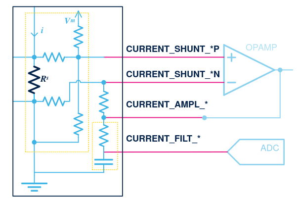
Three shunt resistors are used to measure phase currents (one per phase). These shunts are located on the power board or on the inverter. The circuitry on the control board does not amplify the voltages measured across the shunts. This amplification is performed by op amp peripherals that are provided by the MCU. Rather, the board provides the offset network, the resistors needed to build the amplification gain and a low-pass filter in front of each of the ADC channels used to sample the measured values.
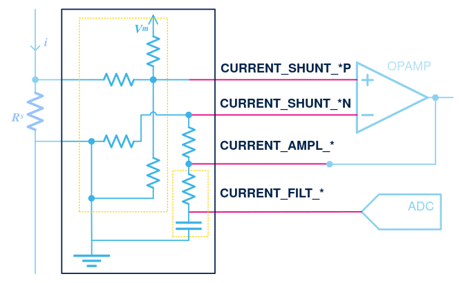
To achieve this, the output pin of the op amp peripherals must differ from that of the ADC peripherals input. See the following figure illustrating this hardware variant. So, this hardware variant defines twelve signals that make all the links with the MCU.
This hardware variant can be used on a control board or on an inverter board. In the case of an inverter, the shunt resistor value is described, as outlined in the following figure.
This hardware variant can also be used on a control board. In that case, the shunt resistor is not implemented on the control board but rather on the power board that must then implement the three-shunt, raw currents, differential op amp hardware variant. The complete implementation of the current sensing feature is spread across the control and the power board. Current sensing signals that are coming from the power stage must be connected to the same MCU pin as the ones listed in the control board with the same name. The following figure depicts this flavor of the hardware variant.
3.1.1.8.2. Properties
| Parameters | Type | Description |
|---|---|---|
shuntResistor
|
Number | Shunt resistor value in Ohm. This parameter is optional. Its presence is mandatory for an inverter board. Its value is ignored for a control board. |
offsetNetworkAttenuation
|
Number | Gain of the offset network |
opAmpGain
|
Number | Gain of the op amp amplification |
polarizationOffset
|
Number | Shift voltage added by the offset network, in Volts, at op amp output. |
amplifyingNetworkImax
|
Number | Maximum current that is measurable by the current sensing network, in Amperes. |
amplifyingNetworkVm
|
Number | Voltage reference of the current sensing network, in Volts |
amplifyingNetworkPrating
|
Number | Rated power (that can go through the shunt resistor), in Watts. |
| Number | low pass filter cutoff pulse in rad/s |
See current sensing signals conditioning model for complete information on the offsetNetworkAttenuation, opAmpGain, and polarizationOffset properties.
3.1.1.8.3. Signals
| Signals | Description |
|---|---|
CURRENT_SHUNT_UP
|
Phase U raw shunt voltage |
CURRENT_SHUNT_VP
|
Phase V raw shunt voltage |
CURRENT_SHUNT_WP
|
Phase W raw shunt voltage |
CURRENT_AMPL_U
|
Phase U amplified shunt voltage (op amp output) |
CURRENT_AMPL_V
|
Phase V amplified shunt voltage (op amp output) |
CURRENT_AMPL_W
|
Phase W amplified shunt voltage (op amp output) |
CURRENT_SHUNT_UN
|
Phase U op amp inverting input. |
CURRENT_SHUNT_VN
|
Phase V op amp inverting input. |
CURRENT_SHUNT_WN
|
Phase W op amp inverting input. |
CURRENT_FILT_U
|
Phase U amplified and filtered voltage (ADC input) |
CURRENT_FILT_V
|
Phase V amplified and filtered voltage (ADC input) |
CURRENT_FILT_W
|
Phase W amplified and filtered voltage (ADC input) |
3.1.2. Single-shunt current sensing
Current sensing feature hardware variants using a single-shunt current sensing topology.
3.1.2.1. Single-shunt, amplified current hardware variant
The type of this hardware variant is SingleShunt_AmplifiedCurrents
This hardware variant is available on power boards and inverter boards.
3.1.2.1.1. Description
One shunt resistor is used to measure phase currents (measurements are made at different instants of the PWM period to get all currents) and the inverter (or the power board) amplifies the voltage measured across the shunt. The signal coming out of the power stage is connected to an ADC on the MCU. The ADC is in single-ended mode and the signal carries the potential on the high side of the shunt resistor, which is then compared to the ground of the MCU. Hence, only one signal is coming out of the power stage for this variant of the feature.
3.1.2.1.2. Properties
| Parameters | Type | Description |
|---|---|---|
shuntResistor
|
Number | Shunt resistor value in Ohm |
offsetNetworkAttenuation
|
Number | Gain of the offset network |
opAmpGain
|
Number | Gain of the op amp amplification |
polarizationOffset
|
Number | Shift voltage added by the offset network, in Volts, at op amp output. |
amplifyingNetworkImax
|
Number | Maximum current that is measurable by the current sensing network. |
amplifyingNetworkVm
|
Number | Voltage reference of the current sensing network |
amplifyingNetworkPrating
|
Number | Rated power (that can go through the shunt resistor) |
See current sensing signals conditioning model for complete information on the offsetNetworkAttenuation, opAmpGain, and polarizationOffset properties.
3.1.2.1.3. Signals
| Signals | Description |
|---|---|
CURRENT_AMPL
|
Amplified shunt voltage |
3.1.2.2. Single-shunt, amplified currents without offset network hardware variant
The type of this hardware variant is SingleShunt_AmplifiedCurrents_noOffset
3.1.2.2.1. Description
One shunt resistor is used to measure phase currents and the power board amplifies the voltage measured across the shunt. However, the current is always positive, so there is no offset circuitry to level it up. The signal coming out of the power board is connected to an ADC on the MCU. The ADC is in single-ended mode and the signal carries the potential on the high side of the shunt resistor, which is then compared to the ground of the MCU. Hence, only one signal is coming out of the power board for this variant of the feature.
3.1.2.2.2. Properties
| Parameters | Type | Description |
|---|---|---|
shuntResistor
|
Number | Shunt resistor value in Ohm |
opAmpGain
|
Number | Gain of the op amp amplification |
amplifyingNetworkImax
|
Number | Maximum current that is measurable by the current sensing network. |
amplifyingNetworkVm
|
Number | Voltage reference of the current sensing network |
amplifyingNetworkPrating
|
Number | Rated power (that can go through the shunt resistor) |
3.1.2.2.3. Signals
| Signals | Description |
|---|---|
CURRENT_AMPL
|
Amplified shunt voltage |
3.1.2.3. Single-shunt, raw currents, single-ended op amp hardware variant
The type of this hardware variant is: SingleShunt_RawCurrents_SingleEnded
This hardware variant is available on power boards.
3.1.2.3.1. Description
One shunt resistor is used to measure phase currents (two measurements are made at different instants of the PWM period to get all currents). The power board does not amplify the voltage measured across the shunt or does it offset it. The signal coming out of the power board must then be connected to an op amp peripheral on the MCU and to an offset network implemented on the control board. The op amp is in single-ended mode and the signal carries the potential on the high side of the shunt resistor, which is then compared to the ground of the MCU. Hence, only one signal is coming out of the power board for this variant of the feature.
This hardware variant can only be found on a power board.
3.1.2.3.2. Properties
| Parameters | Type | Description |
|---|---|---|
shuntResistor
|
Number | Shunt resistor value in Ohm |
3.1.2.3.3. Signals
| Signals | Description |
|---|---|
CURRENT_SHUNT
|
Raw shunt high side potential to be fed into the noninverting input of an op amp |
3.1.2.4. Single-shunt, raw currents, single-ended internal op amp with external gain hardware variant
The type of this hardware variant is: SingleShunt_RawCurrents_SingleEnded_ExternalGain
This hardware variant is available on control boards and inverter boards.
3.1.2.4.1. Description
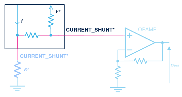
One shunt resistor is used to measure phase currents (two measurements are made at different instants of the PWM period to get all currents). This hardware variant does not amplify the voltage measured across the shunt but it offsets it by a positive shift voltage. It also provides the electronics needed to build the gain of the op amp used for the amplification of the current measurement. The variant provides three signals among which CURRENT_SHUNT that carries the potential on the high side of the shunt resistor offset by the shift voltage. This first signal is used to compute the values of the currents flowing through the phases of the motor. The two others connect the amplifying op amp to the amplification gain circuitry provided by the hardware variant.
The signals coming out of the hardware variant are meant to be connected to an op amp peripheral embedded in the MCU. This op amp is configured in single-ended mode and the amplification gain is built outside of the MCU, in the hardware variant. The op amp noninverting input is connected to the CURRENT_SHUNT signal. Its inverting input is connected to the CURRENT_AMPLN signal and its output is connected to the CURRENT_AMPL signal.
This hardware variant cannot be found on a power board. The following figure sketches an overview of it.
This hardware variant can be used on a control board. In that case, the shunt resistor is not implemented on the control board but rather on the power board that must then implement the single-shunt, raw currents, single-ended op amp hardware variant. The complete implementation of the current sensing feature is spread across the control and the power board. Current sensing signals that are coming from the power stage must be connected to the same MCU pin as the ones listed in the control board with the same name. The following figure depicts this flavor of the hardware variant.
The connection of the CURRENT_SHUNT signal coming from the power board to the proper MCU pin is stated in the terminals object of the connector object in which the hardware variant is described.
3.1.2.4.2. Properties
| Parameters | Type | Description |
|---|---|---|
shuntResistor
|
Number | Shunt resistor value in Ohm. This parameter is optional. Its presence is mandatory for an inverter board. Its value is ignored for a control board. |
offsetNetworkAttenuation
|
Number | Gain of the offset network |
opAmpGain
|
Number | Gain of the op amp amplification |
polarizationOffset
|
Number | Shift voltage added by the offset network, in Volts, at op amp output. |
amplifyingNetworkImax
|
Number | Maximum current that is measurable by the current sensing network. |
amplifyingNetworkVm
|
Number | Voltage reference of the current sensing network |
amplifyingNetworkPrating
|
Number | Rated power (that can go through the shunt resistor) |
See current sensing signals conditioning model for complete information on the offsetNetworkAttenuation, opAmpGain, and polarizationOffset properties.
3.1.2.4.3. Signals
| Signals | Description |
|---|---|
CURRENT_SHUNT
|
Raw shunt voltage to be fed into the noninverting input of an op amp |
CURRENT_AMPL
|
Amplified shunt voltage (op amp output) |
CURRENT_AMPLN
|
Op amp inverting input |
3.1.2.5. Single-shunt, raw currents, single-ended internal op amp with internal gain hardware variant
The type of this hardware variant is: SingleShunt_RawCurrents_SingleEnded_InternalGain
This hardware variant is available on control boards and inverter boards.
3.1.2.5.1. Description
One shunt resistor is used to measure phase currents (two measurements are made at different instants of the PWM period to get all currents). This hardware variant does not amplify the voltage measured across the shunt, but it offsets it by a positive shift voltage. The variant provides one signal — CURRENT_SHUNT — that carries the potential on the high side of the shunt resistor offset by the shift voltage. This signal is used to compute the values of the currents flowing through the phases of the motor.
The signal coming out of the hardware variant is meant to be connected to an op amp peripheral embedded in the MCU. This op amp is configured in single-ended mode and the amplification gain is made in the MCU using the PGA. The op amp noninverting input is connected to the CURRENT_SHUNT signal. The voltage measured between the potential carried by this signal and the ground of the MCU is amplified by the op amp and then fed into an ADC embedded in the MCU.
This hardware variant cannot be found on a power board. The following figure sketches an overview of it.
This hardware variant can be used on a control board. In that case, the shunt resistor is not implemented on the control board but rather on the power board that must then implement the single-shunt, raw currents, single-ended op amp hardware variant. The complete implementation of the current sensing feature is spread across the control and the power board. Current sensing signals that are coming from the power stage must be connected to the same MCU pin as the ones listed in the control board with the same name. The following figure depicts this flavor of the hardware variant.
The connection of the CURRENT_SHUNT signal coming from the power board to the proper MCU pin is stated in the terminals object of the connector object in which the hardware variant is described.
3.1.2.5.2. Properties
| Parameters | Type | Description |
|---|---|---|
shuntResistor
|
Number | Shunt resistor value in Ohm. This parameter is optional. Its presence is mandatory for an inverter board. Its value is ignored for a control board. |
offsetNetworkAttenuation
|
Number | Gain of the offset network |
opAmpGain
|
Number | Gain of the op amp amplification |
polarizationOffset
|
Number | Shift voltage added by the offset network, in Volts, at op amp output. |
amplifyingNetworkImax
|
Number | Maximum current that is measurable by the current sensing network. |
amplifyingNetworkVm
|
Number | Voltage reference of the current sensing network |
amplifyingNetworkPrating
|
Number | Rated power (that can go through the shunt resistor) |
See current sensing signals conditioning model for complete information on the offsetNetworkAttenuation, opAmpGain, and polarizationOffset properties.
3.1.2.5.3. Signals
| Signals | Description |
|---|---|
CURRENT_SHUNT
|
Raw shunt voltage to be fed into the noninverting input of an op amp |
3.1.3. Insulated current sensing
Current sensing feature hardware variants using insulated current sensing.
3.1.3.1. Two ICS currents hardware variant
The type of this hardware variant is: TwoICSCurrents
This hardware variant is available on power boards and inverter boards.
3.1.3.1.1. Description
Two insulated current sensors (Hall effect sensors) are used to measure two phase currents (phases U and V). The signals coming out of the inverter or the power board are connected to ADC peripherals on the MCU. The ADCs are in single-ended mode and the two signals carry the output signals of the Hall sensors. Hence, only two signals are coming out of the power stage for this variant of the feature. Since only two currents are measured, the third needs to be reconstructed thanks to the iu + iv + iw = 0 relation.
3.1.3.1.2. Properties
| Parameters | Type | Description |
|---|---|---|
icsGain
|
Number | Gains of the ICS sensors. |
3.1.3.1.3. Signals
| Signals | Description |
|---|---|
CURRENT_ICS_U
|
Phase U Hall sensor voltage |
CURRENT_ICS_V
|
Phase V Hall sensor voltage |
3.1.4. Current sensing signals conditioning model
There are many ways to implement the circuitry that conditions the shunt voltages before sending them to the ADCs. But all these implementations essentially do the same things: they offset the shunt voltages by a constant shift value and amplify the resulting signals with an op amp. This is done so that the ADCs are presented with positive signals that fit within their acquisition capabilities for the whole range of current values to measure.
The voltage sampled by an ADC is then a linear function of the current to measure as outlined by the figure below.
Current sensing hardware variants describe this affine function with three parameters: * the offset voltage: polarizationOffset * the gain of the op amp circuit: opAmpGain * the gain of the offset circuit: offsetNetworkAttenuation
The following formula gives the voltage acquired by ADCs from the phase current, using these parameters:
VADC = opAmpGain × offsetNetworkAttenuation × Vshunt + polarizationOffset
Where Vshunt is the voltage across the shunt resistor and VADC the voltage acquired by the ADC.
Some current sensing hardware variants provide a rawPolarizationOffset parameter instead of the polarizationOffset one. This is the case for hardware variants that do not implement an op amp but rather rely on op amps embedded in the MCU. Then, since the op amp gain is unknown, the polarization offset does not account for it. The formula giving the voltage acquired by the ADCs then becomes:
VADC = OpAmpGain × (offsetNetworkAttenuation × Vshunt + rawPolarizationOffset)
Where OpAmpGain is the gain of the internal op amp.
3.2. Speed and position sensing
This feature aims at measuring or estimating the speed and the position of the rotor of a motor.
The type of this feature is SpeedAndPositionSensing.
This feature does not define any global property.
The following sections specify the hardware variants of this feature.
3.2.1. Back-EMF sensing with ADC hardware variant
The type of this hardware variant is BEMFSensingADC
3.2.1.1. Description
The back-EMF value is measured on each motor phase when the PWM output of that phase is floating. The signal (divided or not divided by a resistor network enabled by a GPIO) is to be acquired by an ADC.
3.2.1.2. Properties
| Parameters | Type | Description |
|---|---|---|
dividingNetworkR1
|
Number | Value of resistance R1 of the BEMF sensing dividing network enabled by signal BEMF_DIVIDER GPIO
|
dividingNetworkR2
|
Number | Value of resistance R2 of the BEMF sensing dividing network enabled by signal BEMF_DIVIDER GPIO
|
3.2.1.3. Signals
| Signal | Description |
|---|---|
BEMF_U
|
Phase U back-EMF signal |
BEMF_V
|
Phase V back-EMF signal |
BEMF_W
|
Phase W back-EMF signal |
BEMF_DIVIDER
|
Output signal to enable dividing network during PWM on-time sensing. |
3.2.2. Hall effect sensor hardware variant
The type of this hardware variant is HallEffectSensor
3.2.2.1. Description
Three Hall effect sensors are used on the motor to measure the position of the rotor. The actual rotor position is known six times in a rotation, at six fixed and evenly spread angular positions. Such sensors output three signals that must be connected to channels 1, 2, and 3 of a general-purpose timer that supports Hall sensor decoding (usually TIM2, TIM3, TIM4, and TIM5).
3.2.2.2. Properties
None.
3.2.2.3. Signals
| Signal | Description |
|---|---|
HALLSENSOR_H1
|
Hall sensor signal 1. |
HALLSENSOR_H2
|
Hall sensor signal 2. |
HALLSENSOR_H3
|
Hall sensor signal 3. |
3.2.3. Relative quadrature encoder hardware variant
The type of this hardware variant is QuadratureEncoderRelative
3.2.3.1. Description
A quadrature encoder is used on the motor to measure changes in the position of the rotor (the speed). The encoder outputs two signals that indicate when the rotor has rotated by one encoder angular step and also in which direction. These two signals must be connected to channels 1 and 2 of a general-purpose timer that supports quadrature encoder decoding (usually TIM2, TIM3, TIM4, and TIM5).
3.2.3.2. Properties
None.
3.2.3.3. Signals
| Signal | Description |
|---|---|
QENC_A
|
Quadrature encoder signal A |
QENC_B
|
Quadrature encoder signal B |
3.2.4. Absolute quadrature encoder hardware variant
The type of this hardware variant is QuadratureEncoderAbsolute
3.2.4.1. Description
A quadrature encoder is used on the motor to measure changes in the position of the rotor (the speed). It is similar to QuadratureEncoderRelative except that it provides an additional signal that triggers once per rotation, and then indicates an absolute position. The actual position is then known once the additional signal has been triggered. This kind of encoder outputs three signals that indicate when the rotor has rotated by one encoder angular step, in which direction, and also the absolute position once per rotation. The first two signals, QENC_A and QENC_B must be connected to channels 1 and 2 of a general-purpose timer that supports quadrature encoder decoding (usually TIM2, TIM3, TIM4, and TIM5). The last signal, QENC_Z can be connected to any GPIO.
3.2.4.2. Properties
None.
3.2.4.3. Signals
| Signal | Description |
|---|---|
QENC_A
|
Quadrature encoder signal A |
QENC_B
|
Quadrature encoder signal B |
QENC_Z
|
Quadrature encoder signal Z (Absolute position signal) |
3.2.5. Back-EMF sensing with ADC and fixed divider hardware variant
The type of this hardware variant is BEMFSensingADCFixedDivider.
3.2.5.1. Description
The back-EMF value is measured on each motor phase when the PWM output of that phase is floating. The signal (divided by a resistor network) is to be acquired by an ADC.
3.2.5.2. Properties
| Parameters | Type | Description |
|---|---|---|
dividingNetworkR1
|
Number | Value of resistance R1 of the BEMF sensing dividing network enabled by signal BEMF_DIVIDER GPIO
|
dividingNetworkR2
|
Number | Value of resistance R2 of the BEMF sensing dividing network enabled by signal BEMF_DIVIDER GPIO
|
3.2.5.3. Signals
| Signal | Description |
|---|---|
BEMF_U
|
Phase U back-EMF signal |
BEMF_V
|
Phase V back-EMF signal |
BEMF_W
|
Phase W back-EMF signal |
3.3. Phase voltage generation
This feature provides the voltages to apply to the phases of a motor to drive it. These voltages are produced from a DC bus and their values are driven by voltage references output by the MCU.
The type of this feature is PhaseVoltageGeneration.
This feature defines the following properties:
| Parameters | Type | Description |
|---|---|---|
driverName
|
String | Driver or IGBT or MOSFET name |
driverPN
|
String | Driver or IGBT or MOSFET part number |
useSTGAP1S
|
Bool | whether STGAP1S intelligent gate driver. Defaults to false.
|
tNoise
|
Number | TNoise parameter of the switches. In ns |
minDeadTime
|
Number | Min dead-time, in ns. If the parameter is not applicable to a driver, its value should be set to 0. |
maxSwitchingFreq
|
Number | Max switching frequency, in kHz |
The following sections specify the hardware variants of this feature.
3.3.1. Driving high and low sides hardware variant
The type of this hardware variant is DrivingHighAndLowSides
3.3.1.1. Description
Both the high- and low-side power switches that connect each phase of the motor to Vbus and the ground need to be driven by the MCU. This results in six signals exchanged between the power stage and the MCU. These signals must be connected to the TIM_CHx and TIM_CHxN pins of one advanced timer of the MCU, with x being 1, 2, or 3:
- The high-side signals are to be connected to
TIM_CHxpins. - The low-side signals are to be connected to
TIM_CHxNpins. - Phase U signals are connected to
TIM_CH1andTIM_CH1Npins. - Phase V signals are connected to
TIM_CH2andTIM_CH2Npins. - Phase W signals are connected to
TIM_CH2andTIM_CH2Npins.
All the signals must be connected to the same timer peripheral.
3.3.1.2. Properties
| Parameters | Type | Description |
|---|---|---|
deadTime
|
Number | Dead time to insert when switching between high-sides and low-sides. |
highSideSwitchesDrivingPolarity
|
String | Polarity of the driving signals for the high-side switches. This is an enumeration in which possible values are: “Active low” or “Active high”.
|
lowSideSwitchesDrivingPolarity
|
String | Polarity of the driving signals for the low-side switches. This is an enumeration in which possible values are: “Active low” or “Active high”.
|
3.3.1.3. Signals
| Signal | Description |
|---|---|
PWM_CHU_H
|
Phase U high side switch drive |
PWM_CHV_H
|
Phase V high side switch drive |
PWM_CHW_H
|
Phase W high side switch drive |
PWM_CHU_L
|
Phase U low side switch drive |
PWM_CHV_L
|
Phase V low side switch drive |
PWM_CHW_L
|
Phase W low side switch drive |
3.3.2. Driving high sides and three enables hardware variant
The type of this hardware variant is DrivingHighSidesAndThreeEnables
3.3.2.1. Description
Only the high-side switches that connect each phase of the motor to Vbus need to be driven by the MCU. The low-side switches that connect each phase of the motor to the ground are automatically handled by the driver on the power stage. Additionally, the driving of each phase is subject to an enable signal. This results in six signals exchanged between the power stage and the MCU: three signals that enable the driving of each phase and three signals to drive each phase.
The three high-side signals must be connected to the TIM_CH1 (phase U), TIM_CH2 (phase V), and TIM_CH3 (phase W) pins of the same timer. This timer peripheral must be the same for the three signals and it must provide the PWM feature.
The three enable signals can be connected to any GPIO of the MCU.
3.3.2.2. Properties
| Parameters | Type | Description |
|---|---|---|
deadTime
|
Number | Dead time to insert when switching between high-sides and low-sides. |
highSideSwitchesDrivingPolarity
|
String | Polarity of the driving signals for the high-side switches. This is an enumeration in which possible values are: “Active low” or “Active high”.
|
enableDrivingPolarity
|
String | Polarity of the enable signals. This is an enumeration in which possible values are: “Active low” or “Active high”.
|
3.3.2.3. Signals
| Signal | Description |
|---|---|
PWM_CHU_H
|
Phase U switch drive |
PWM_CHV_H
|
Phase V switch drive |
PWM_CHW_H
|
Phase W switch drive |
PWM_CHU_EN
|
Phase U enable |
PWM_CHV_EN
|
Phase V enable |
PWM_CHW_EN
|
Phase W enable |
3.3.3. Driving high sides and one enable hardware variant
The type of this hardware variant is: DrivingHighSidesAndOneEnable.
3.3.3.1. Description
Only the high side switches that connect each phase of the motor to Vbus need to be driven by the MCU. The low side switches that connect each phase of the motor to the ground are automatically handled by the driver on the power stage. Additionally, the driving of all phases is subject to an enable signal. This results in four signals exchanged between the power stage and the MCU: one signal that enables the driving of the phases and three signals to actually drive each phase.
The three high side signals must be connected to the TIM_CH1 (phase U), TIM_CH2 (phase V) and TIM_CH3 (phase W) pins of the same timer. This timer peripheral must be the same for the three signals and it must provide the PWM feature.
The enable signal can be connected to any GPIO of the MCU.
3.3.3.2. Properties
| Parameters | Type | Description |
|---|---|---|
deadTime
|
Number | Dead time to insert when switching between high-sides and low-sides. |
highSideSwitchesDrivingPolarity
|
String | Polarity of the driving signals for the high-side switches. This is an enumeration in which possible values are: “Active low” or “Active high”.
|
enableDrivingPolarity
|
String | Polarity of the enable signal. This is an enumeration in which possible values are: “Active low” or “Active high”.
|
3.3.3.3. Signals
| Signal | Description |
|---|---|
PWM_CHU_H
|
Phase U switch drive |
PWM_CHV_H
|
Phase V switch drive |
PWM_CHW_H
|
Phase W switch drive |
PWM_EN
|
Driver enable |
3.3.4. Driving high and low sides power switches hardware variant
The type of this hardware variant is PoweringHighAndLowSides
3.3.4.1. Description
Both the high- and the low-side power switches that connect each phase of the motor to Vbus and the ground need to be driven. The MCU commands the six switches of a driver that will finally drive the power switches connected to the motor phases. This results in six signals exchanged between the power stage and the control stage. These signals must be connected to the six outputs of the driver coming from the control stage on one side and to the six power switches featured on the power stage on the other side.
An example of usage of this hardware variant is with a hardware configuration that uses STSPIN332G4 or STSPIN32F0 devices that embed the phases driver in the same package as the MCU.
3.3.4.2. Properties
| Parameters | Type | Description |
|---|---|---|
deadTime
|
Number | Dead time to insert when switching between high-sides and low-sides. |
highSideSwitchesDrivingPolarity
|
String | Polarity of the driving signals for the high-side switches. This is an enumeration in which possible values are: “Active low” or “Active high”.
|
enableDrivingPolarity
|
String | Polarity of the enable signals. This is an enumeration in which possible values are: “Active low” or “Active high”.
|
3.3.4.3. Signals
| Signal | Description |
|---|---|
GD_CHU_H
|
Phase U high side power switch drive |
GD_CHV_H
|
Phase V high side power switch drive |
GD_CHW_H
|
Phase W high side power switch drive |
GD_CHU_L
|
Phase U low side power switch drive |
GD_CHV_L
|
Phase V low side power switch drive |
GD_CHW_L
|
Phase W low side power switch drive |
3.4. Motor phases voltage sensing
This feature aims at measuring the voltages present on the phases of a motor. In principle, it is very close to what some implementations of the speed and position sensing feature, like the Back-EMF sensing with ADC do. However, the purpose and the actual implementation may differ a lot.
The type of this feature is: PhaseVoltageSensing.
This feature does not define any global property.
The following sections specify the hardware variants of this feature.
3.4.1. Three phase voltage dividers, filtered hardware variant
The type of this hardware variant is: ThreePhaseVoltageDividersFiltered.
3.4.1.1. Description
Three voltage dividers are used to measure the phases voltages (one per phase). The signals coming out of the divider is low-pass filtered and then connected to ADC peripherals on the MCU. The ADCs are in single-ended mode and the voltage signals are compared to the ground of the MCU.
3.4.1.2. Properties
| Parameters | Type | Description |
|---|---|---|
voltageDividerValue |
Number | Value of the voltage divider |
cutoffPulse |
Number | low pass filter cutoff pulse in rad/s |
3.4.1.3. Signals
| Signal | Description |
|---|---|
VOLTAGE_DIV_FILT_U |
Phase U voltage, divided and low-pass filtered |
VOLTAGE_DIV_FILT_V |
Phase V voltage, divided and low-pass filtered |
VOLTAGE_DIV_FILT_W |
Phase W voltage, divided and low-pass filtered |
3.5. Driver protection
This feature provides the reporting of error conditions occurring on gate drivers controlled by the MCU.
The type of this feature is: DriverProtection.
This feature does not define any global property.
The following sections specify the hardware variants of this feature.
3.5.1. Single error trigger hardware variant
The type of this hardware variant is: SingleErrorTrigger_FixedReference.
This hardware variant is available on power boards and on inverter boards.
3.5.1.1. Description
Error conditions are detected on the power stage (by an integrated driver for instance) and relayed to the MCU through a single signal. This signal is usually connected to a break input of the timer peripheral (BREAKIN or BREAKIN2) used to generate the PWM driving the phases of the motor. When the trigger is asserted, the MCU can take an appropriate measure to protect.
3.5.1.2. Properties
| Parameters | Type | Description |
|---|---|---|
DPSignalPolarity |
String | Error trigger feedback signal polarity enumeration. Possible values are: "Active low" or "Active high".
|
DPTriggerFilterDuration |
Number | Duration of the filter preventing spurious triggers in ns. Set to 0 if not filter is required. |
3.5.1.3. Signals
| Signal | Description |
|---|---|
DP_TRIGGER |
Error condition trigger. This signal is usually connected to a break input of the timer peripheral (BREAKIN or BREAKIN2).
|
3.6. Over current protection
This feature provides the capability to detect overcurrent conditions on the phases of a motor and to report them to the MCU.
The type of this feature is OverCurrentProtection.
This feature does not define any global property.
The following sections specify the hardware variants of this feature.
3.6.1. On power stage over current protection hardware variant
The type of this hardware variant is OnPowerStageOCP.
This hardware variant is available on power boards and inverter boards.
3.6.1.1. Description
Overcurrent conditions are detected on the power stage (by an integrated driver for instance) and relayed to the control stage through a single signal. This signal is usually connected to a break input of the timer peripheral used to generate the PWM driving the phases of the motor.
3.6.1.2. Properties
| Parameters | Type | Description |
|---|---|---|
OCThreshold
|
Number | Overcurrent threshold in Amperes. |
OCNetworkGain
|
Number | Overcurrent network gain in V/A. |
OCNetworkOffset
|
Number | Overcurrent network offset in Volts. |
OCComparatorThreshold
|
Number | Overcurrent comparator threshold in Volts. |
OCSignalPolarity
|
String | Overcurrent feedback signal polarity enumeration. Possible values are: “Active low” or “Active high”
|
3.6.1.3. Signals
| Signal | Description |
|---|---|
OC_TRIGGER
|
Overcurrent protection condition trigger. |
3.6.2. Single input, raw currents protection, internal reference hardware variant
The type of this hardware variant is SingleInput_RawCurrents_Protection_IntRef.
This hardware variant is available on control boards, power boards, and inverter boards.
3.6.2.1. Description
Overcurrent conditions are detected on the MCU thanks to a single internal comparator. To that end, the power stage conditions the current it senses into a single analog signal that fits in the ranges accepted by the internal comparator. This signal is then connected to the noninverting input of an internal comparator of the MCU. The reference of the comparator is generated internally by the MCU (with an internal DAC connection for instance) based on the parameters of the hardware variant.
3.6.2.2. Properties
| Parameters | Type | Description |
|---|---|---|
OCNetworkGain
|
Number | Overcurrent network gain in V/A. |
OCNetworkOffset
|
Number | Overcurrent network offset in Volts. |
OCComparatorThreshold
|
Number | Overcurrent comparator threshold in Volts. |
OCSignalPolarity
|
String | Overcurrent feedback signal polarity enumeration. Possible values are: “Active low” or “Active high”.
|
3.6.2.3. Signals
| Signal | Description |
|---|---|
CURRENT_INPUT_P
|
Conditioned analog signal representing the current. This signal is fed into a comparator of the MCU. |
3.7. Inrush current limiter
This feature aims at limiting the inrush current at startup.
The type of this feature is ICL.
This feature does not define any global property.
The following sections specify the hardware variants of this feature.
3.7.1. Switched resistor inrush current limiter hardware variant
The type of this hardware variant is InrushCurrentLimiter.
3.7.1.1. Description
A resistor is used to limit the current that can flow into the power stage of the motor drive at startup. When active, this resistor is in series with the circuitry it protects. The feature is enabled and disabled by a switch that is controlled by the MCU through a signal that can be connected to any GPIO of the MCU.
3.7.1.2. Properties
| Parameter | Type | Description |
|---|---|---|
switchPolarity
|
String | Polarity of the ICL driving switch. This is an enumeration. Possible values are: “Active low” or “Active high”.
|
capsChargingDelay
|
Number | Duration of the charging of the boot capacitors. This indicates the minimum time during which the ICL must remain active. |
3.7.1.3. Signals
| Signal | Description |
|---|---|
ICL_ENABLE
|
ICL enable signal. |
3.8. Motor Brake
This feature brakes the motor rotor.
The type of this feature is Brake.
This feature does not define any global property.
The following sections specify the hardware variants of this feature.
3.8.1. Dissipative brake hardware variant
The type of this hardware variant is DissipativeBreak
3.8.1.1. Description
A braking resistor is used to dissipate the electric energy generated by the motor when it decelerates. This braking resistor is not connected unless the brake is activated. This is done with a signal that can be connected to any GPIO of the MCU.
3.8.1.2. Properties
| Parameters | Type | Description |
|---|---|---|
rBrakeEnableSignalPolarity
|
String | Polarity of the signal enabling the resistive break. This is an enumeration. Possible values are: “Active low” or “Active high”
|
3.8.1.3. Signals
| Signal | Description |
|---|---|
RBRAKE_ENABLE
|
Brake resistor trigger. |
3.9. Current limiter
This feature aims at limiting the current that flows into the phases of a BLDC motor. It is usually used where the motor is driven with the six-step technique.
The type of this feature is CurrentLimiter.
This feature does not define any global property.
The following sections specify the hardware variants of this feature.
3.9.1. PWM external current limiter hardware variant
The type of this hardware variant is ExternalCurrentLimiter_PWM.
This hardware variant is available on power boards, and inverter boards.
3.9.1.1. Description
The current limit reference is a PWM signal, generated from the MCU by a timer peripheral. The PWM signal is low pass filtered and fed into a comparator, located on the board, that compares it to the phase current measurement. The output signal of the comparison is connected to the MCU.
When the measured current gets too high, the MCU stops the motor-phase-voltage generation. When the measured current goes lower than the reference, the MCU resumes motor-phase voltage generation. Usually, the comparison output signal is connected to the ETR (external trigger) input of the timer used for motor-phase voltage generation.
3.9.1.2. Properties
| Parameter | Type | Description |
|---|---|---|
PWMDefaultFreq
|
Number | The recommended (maximum) frequency of the PWM reference signal, in Hz. Linked to the cutoff frequency of the low-pass filter. |
PWMRefDivider
|
Number | TBD |
ETRPolarity
|
String | Polarity of the external trigger signal of the timer. This is an enumeration in which possible values are: “Active low” or “Active high”.
|
3.9.1.3. Signals
| Signal | Description |
|---|---|
PWM_REF
|
Current limit reference PWM signal |
HF_ETR
|
Phase-voltage generation hold trigger. |
3.9.2. PWM internal current limiter hardware variant
The type of this hardware variant is InternalCurrentLimiter_PWM_IntRef.
This hardware variant is available on power boards, and inverter boards.
3.9.2.1. Description
The current limit reference is a PWM signal, generated from the MCU by a timer peripheral. The PWM signal is low pass filtered, added to the phase current, and fed into an MCU internal comparator.
The output signal of the comparison is connected to the MCU.
When the measured current gets too high, the MCU stops the motor-phase-voltage generation. When the measured current goes lower than the reference, the MCU resumes motor-phase voltage generation. Usually, the comparison output signal is connected to the ETR (external trigger) input of the timer used for motor-phase-voltage generation.
3.9.2.2. Properties
| Parameter | Type | Description |
|---|---|---|
PWMDefaultFreq
|
Number | The recommended (maximum) frequency of the PWM reference signal, in Hz.
Linked to the cutoff frequency of the low-pass filter. |
PWMRefDivider
|
Number | TBD |
CLComparatorThreshold
|
Number | Threshold of the comparator connected to the ETR. |
ETRPolarity
|
String | Polarity of the external trigger signal of the timer. This is an enumeration in which possible values are: “Active low” or “Active high”.
|
3.9.2.3. Signals
| Signal | Description |
|---|---|
PWM_REF
|
Current limit reference signal |
CURRENT_AMPL_PLUS_PWM_REF
|
signal fed into the comparator. |
3.10. Bus voltage measurement
This feature provides the capability to measure the voltage on the bus.
The type of this feature is VBusSensing.
This feature does not define any global property.
The following sections specify the hardware variants of this feature.
3.10.1. VBus sensing hardware variant
The type of this hardware variant is VBusSensing
3.10.1.1. Description
The voltage on the high side of the bus goes through a divider and can be fed into an ADC channel configured in single-ended mode. The electrical ground is shared with the MCU.
3.10.1.2. Properties
| Parameter | Type | Description |
|---|---|---|
busVoltageDivider
|
Number | Bus voltage sensing divider |
busvoltageDividerR1
|
Number | Value of resistance R1 of the bus voltage measurement network. |
busvoltageDividerR2
|
Number | Value of resistance R2 of the bus voltage measurement network. |
busvoltageDividerR3
|
Number | Value of resistance R3 of the bus voltage measurement network. The use of this resistance is optional. If it is not used, its value is null. |
3.10.1.3. Signals
| Signal | Description |
|---|---|
VBUS
|
Bus voltage measurement |
3.11. Temperature measurement
This feature provides the capability to measure the temperature of the power stage.
The type of this feature is TemperatureSensing.
This feature does not define any global property.
The following sections specify the hardware variants of this feature.
3.11.1. Negative temperature coefficient thermistor hardware variant
The type of this hardware variant is NTCThermistor
3.11.1.1. Description
A negative temperature coefficient thermistor in series with a resistor and plugged into a voltage source is placed near the power drivers. It is used to measure the temperature of the power stage thanks to a signal that carries a voltage proportional to the temperature. This signal can be fed into an ADC channel configured in single-ended mode. The electrical ground is shared with the MCU.
3.11.1.2. Properties
| Parameter | Type | Description |
|---|---|---|
v0
|
Number | V0 reference point of NTC thermistor, in mV |
t0
|
Number | T0 reference point of NTC thermistor, in °C (Celsius degrees) |
ntcThermistorGain
|
Number | Thermistor gain in mV/°C. |
maxSensorTemperature
|
Number | Max working temperature on the sensor, in °C |
3.11.1.3. Signals
| Signal | Description |
|---|---|
TEMPERATURE_NTC
|
Voltage delivered by the thermistor from the MCU ground. |
3.12. Serial port communication
This feature provides a serial port interface allowing the MCU to send and receive data.
The type of this feature is SerialPortCommunication.
This feature does not define any global property.
The following sections specify the hardware variants of this feature.
3.12.1. Two-wire UART communication hardware variant
The type of this hardware variant is Uart2WiresCommunication.
3.12.1.1. Description
A universal synchronous/asynchronous receiver transmitter interface using two wires: Tx and Rx (so without flow control). These two wires are represented by two signals that need to be connected to the Tx and Rx pins of one U(S)ART on the MCU.
3.12.1.2. Properties
None.
3.12.1.3. Signals
| Signal | Description |
|---|---|
UART_TX
|
Transmission line (from MCU to outside) |
UART_RX
|
Reception line (from outside to MCU) |
3.13. Potentiometer
This feature provides a potentiometer that can be read by the MCU.
The type of this feature is Potentiometer.
This feature does not define any global property.
The following sections specify the hardware variants of this feature.
3.13.1. Potentiometer hardware variant
The type of this hardware variant is Potentiometer
3.13.1.1. Description
A potentiometer that delivers a voltage between two limits depending on the settings of the user. The voltage is fed into an ADC.
3.13.1.2. Properties
| Parameter | Type | Description |
|---|---|---|
potVm
|
Number | Voltage reference of the potentiometer |
potRmax
|
Number | Maximum resistance of the potentiometer |
potLevelMin
|
Number | Minimum level of the potentiometer (from 0 to 1) |
3.13.1.3. Signals
| Signal | Description |
|---|---|
POTENTIOMETER_LEVEL
|
Potentiometer output level |
3.14. Button
This feature provides a button that users can activate to provide a boolean input to the MCU. Buttons allow for switching between two states.
The type of this feature is Button.
This feature does not define any global property.
The following sections specify the hardware variants of this feature.
3.14.1. Push button hardware variant
The type of this hardware variant is PushButton
3.14.1.1. Description
A switch that changes position when depressed, and that returns to a stable position when released. The status of the switch is transported by a signal that can be connected to any GPIO.
3.14.1.2. Properties
| Parameter | Type | Description |
|---|---|---|
buttonTriggerEdge
|
String | Edge on which the button triggers (either rising or falling). This is an enum whose possible values are: “Rising Edge” or “Falling Edge”
|
buttonGpioConfig
|
String | Configuration of the pull resistor connected to the GPIO pin used for the button. This is an enum whose possible values are: “No Pull up - No Pull down”, “Pull up” or “Pull down”.
|
3.14.1.3. Signals
| Signal | Description |
|---|---|
BUTTON_TRIGGER
|
Button trigger signal. |
4. Connectors
4.1. Morpho 64 connector
There are several morpho connectors. The most used one, when it comes to motor control, is the “Morpho 64” found on NUCLEO-64 boards. This is the one that is considered here under the morpho type.
It is a 76-pin connector made of two dual-strip physical connectors, usually named CN7 and CN10 (but not always).
The pinning of morpho connectors is not fixed as they are mounted on boards that target many other applications than motor control, and there exist other morpho connectors like the “Morpho 144” one found on bigger Nucleo boards (meaning the F746 Nucleo-144 board). So, it is needed to provide a coherent and unique naming for these pins. As far as motor control is concerned, the pins of the connector are named MRx and MLx where x ranges from 1 to 38. MLx refers to the left physical connector (usually CN7) while MRx refers to the right physical connector (usually CN10). Left and right are determined by holding the board so that the physical connectors are vertical with pin 1 of each being at the top left corner of each connector.
The following figure shows the topology of this connector and the naming of its terminals. These names are used to refer to the terminals of this connector in pin and terminal objects.
4.2. Motor-control connector
The motor-control connector is a 34-pin connector with a fixed assignment. It is identified by the MotorControlConnector type. The following table depicts the topology of this connector and shows the assignment of signals to terminals.
| Terminals | Signals | Signals | Terminals |
|---|---|---|---|
| MC1 | OC_TRIGGER
|
GND | MC2 |
| MC3 | PWM_CHU_H
|
GND | MC4 |
| MC5 | PWM_CHU_L, PWM_CHU_EN
|
GND | MC6 |
| MC7 | PWM_CHV_H
|
GND | MC8 |
| MC9 | PWM_CHV_L, PWM_CHV_EN
|
GND | MC10 |
| MC11 | PWM_CHW_H
|
GND | MC12 |
| MC13 | PWM_CHW_L, PWM_CHU_EN
|
VBUS
|
MC14 |
| MC15 | CURRENT_AMPL_U, CURRENT_SHUNT_U, CURRENT_ICS_U
|
GND | MC16 |
| MC17 | CURRENT_AMPL_V, CURRENT_SHUNT_V, CURRENT_ICS_V, CURRENT_SHUNT
|
GND | MC18 |
| MC19 | CURRENT_AMPL_W, CURRENT_SHUNT_W, CURRENT_ICS_W
|
GND | MC20 |
| MC21 | ICL_TRIGGER
|
GND | MC22 |
| MC23 | RBRAKE_TRIGGER
|
GND | MC24 |
| MC25 | +5 V | TEMPERATURE_NTC
|
MC26 |
| MC27 | PFC_SYNC
|
3.3 V power | MC28 |
| MC29 | PFC_PWM
|
PFC_DISABLE
|
MC30 |
| MC31 | HALLSENSOR_H1, QENC_A
|
PFC_VAC
|
MC32 |
| MC33 | HALLSENSOR_H2, QENC_B
|
HALLSENSOR_H3, QENC_Z
|
MC34 |
