This article provides explanations on how the STM32U0 battery less demo works and describes step-by-step how to reproduce it.
1. Presentation of the demo
1.1. Purpose
The aim of this demo is to illustrate the STM32U0's best-in-class ultra-low-power capabilities. It is running without battery thanks to Dracula technologies inkjet Printed Organic Photovoltaic module, which harvests energy for the STM32U0 MCU. This is a luxmeter and thermometer demo with data being displayed on an LCD segment display, and with the possibility to share measured data wirelessly.
1.2. Configurations
This demo can be configured in two versions.
- The first one is referred as the Data logger only configuration. It consists of one STM32U083C-Discovery kit powered by one Layer photovoltaic module. Every second, the measured temperature or illuminance is displayed on the LCD segment display. By pressing the joystick blue hat of the discovery kit, the user can change which data is being displayed.
- The second one is referred as the Data logger & RF configuration. It consists of two modules, the Data logger & Transmitter module, and the Receiver & Display module.
- The first one is based on the first configuration of the demo, on top of which an X-Nucleo-S2868A2, an RF expansion board, is plugged. In addition to measuring temperature and illuminance, and displaying one of the two measures on the LDC segment display, it sends each second the two measures thanks to the RF module.
- The second one is a module which receives the data and displays it on an LCD screen. It is based on a Nucleo-U083RC on top of which two expansion kits, an X-Nucleo-S2868A2, to receive the data, and an X-Nucleo-GFX01M2, with the LCD screen, are plugged. The two received measures are displayed in real time on the LCD screen, and variations are shown live on a graph chart. This module needs external power supply, such as USB.
2. How the demo works
2.1. Schematics
The figure below shows schematics of the Data logger only configuration on the left, and of the Data logger & RF configuration on the right.
2.2. Demo principle
2.2.1. Overall principle
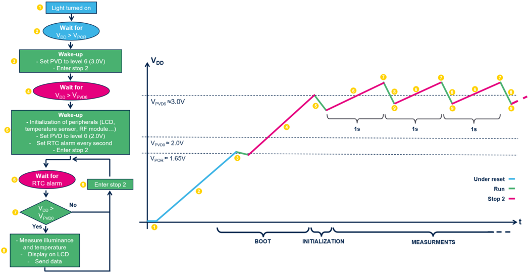
The following flowchart and graph describe the three main phases of the Data logger module: the boot phase, the initialization phase, and the measurement phase.
After connecting the panel, the capacitor starts to charge (1). When voltage first reaches the POR voltage (1.65 V) (2), only the minimum instructions are done before entering stop 2 mode, to consume as little energy as possible. Hence, in this time frame, only PVD is set to level 6 to wake up the STM32U0 when voltage reach 3.0 V (3). This is the critical part of the initialization.
Once the voltage reaches 3.0 V for the first time (4), the initialization of the peripherals can start (5). GPIOs, LCD, ADC, communication with the temperature sensor, and, if present, communication with the RF module is initialized. PVD is set to level 0 (2.0 V). It is used to check that voltage is high enough before starting the measurement and sending process. It is set to this level to have the largest working range. RTC is also configured to wake-up the MCU every second. Then, the MCU enters stop 2 mode until wake-up from RTC (6).
At wake-up, and after checking voltage is high enough (7), the measurement phase is entered (8). Temperature is measured by the STT22H temperature sensor included in the discovery kit. Light is measured by measuring voltage provided by the panel, as explained in the following part. If the RF module is present, measured data is sent. The last step is to enter stop 2 again to harvest energy from the photovoltaic module (9).
2.2.2. State machine during measurement phase
The following state machine describes the different states of algorithm during the main phase of the program, the measurement phase.
2.3. Illuminance measurement
The figure below illustrates the flow of current outside of the illuminance measurement phase. PA0 is in open drain output high configuration, so current flows to the capacitor and the STM32U0.
The illuminance is deduced from the current supplied by the photovoltaic module as both are proportional. The current supplied by the photovoltaic module is deduced by measuring the voltage across the photovoltaic cell when its current is flowing through a resistor only. This voltage is measured by one of the ADC of the STM32U0.
So, the following formula is used to deduce illuminance from the measured ADC voltage:
Where:
is the ambient illuminance.
is the current provided by the photovoltaic module.
is the voltage measured by the ADC.
is a proportionality constant.
is the value of resistor R1.
To have the current of the photovoltaic module to flow through only, PA0 is configured in open drain output low, and a diode isolates the photovoltaic cell and the resistor from the capacitor. The figure below illustrates the flow of current during the illuminance measurement phase.
3. How to reproduce
3.1. Bill of material
Data logger & Transmission module
- 1x STM32U083C Discovery kit (MB1933 revision B)
- 1x Layer® inkjet Printed Organic photovoltaic product from Dracula Technologies
- 1x diode
- 1x 100 µF capacitor
- 1x 2.2 kΩ resistor
- 1x X-Nucleo-S2868A2 (MB1933 revision B)
- 1x 300 kΩ resistor
Receiver & Display module
- 1x Nucleo-U083RC (MB1932 revision B)
- 1x X-Nucleo-S2868A2 (MB1933 revision B)
- 1x X-Nucleo-GFX01M2 (XS2868V2)
- 2x SSQ-119-03-T-D
3.2. Hardware
3.2.1. Reproduction of the Data logger & Transmission module
The figure below shows the modifications to be done on the front side of STM32U083-DK.
- 1. Remove JP5.
- 2. Close JP6 to connect the two right pins of the jumper (supply the temperature sensor by VDD_MCU).
- 3. Remove JP7.
- 4. Remove R57.
- 5. Connect the 100 µF capacitor in the dedicated slot of the DK.
The figure below shows the connections to be done on the bottom side of STM32U083-DK.
- 6. Close SB17.
- 7. Connect PV- to battery– pin.
- 8. Connect PV+ to CN7-38 (PC1).
- 9. Connect the diode between CN7-38 (PC1) and battery+ pin.
The figure below shows the modifications to be done on the front side of X-Nucleo-S2868A2. Another reference picture for the modification is further down in section 3.3.1.1.
- 10. Connect the 2.2 kΩ resistor between A4 (PC1) and A0 (PA0).
- 11. Connect the 300 kΩ pull-up resistor between VREF (CN5-3) and D7 (CN9-8).
- 12. Remove JP1.
The figure below shows the modifications to be done on the bottom side of X-Nucleo-S2868A2.
- 13. Cut CN9-9 and CN9-10.
- 14. Connect CN5-8 to JP1-1.
- 15. Remove R12.
- 16. Plug the X-Nucleo-S2868A2 on the DK's Arduino connectors.
3.2.2. Reproduction of the Receiver & Display module
The figure below shows modifications to be done on the X-Nucleo-S2868A2.
The following solder bridges must be opened.
- A1. R10 - Disconnect SDN from D7.
- A2. R11 - Disconnect SPI SCLK from D3.
- A3. R12 - Disconnect GPIO0 from A0.
- A4. R13 - Disconnect CSN from A1.
- A5. R14 - Disconnect GPIO1 from A2.
- A6. R15 - Disconnect GPIO2 from A3.
- A7. R16 - Disconnect GPIO3 from A5.
The following solder bridges must be closed.
- B1. R6 - Connect SPI SCLK to D13.
- B2. R9 - Connect CSN to D10.
- B3. R18 - Connect GPIO0 to A4.
- B4. CN9-3 on R19 (or R10) - Connect SDN to D2. [1]
The figure below shows the connections and the modification to be done on the Nucleo-U083RC:
- C1. Cut CN7-36 (conflict on this pin between the two extension kits).
- C2. Plug the 2 SSQ-119-03-T-D 19x2 connectors on Nucleo-connectors.
- C3. Plug the X-Nucleo-S2868A2 on Arduino-connectors.
- C4. Plug the X-Nucleo-GFX01M2 on the SSQ-119-03-T-D connectors.
3.3. Software projects
The full project includes three sub-projects:
- The Data-Logger-and-Transmission-Module folder, containing full software project and a ready-to-flash binary file.
- The Receiver-and-Display-Module folder, containing the full software project, expect one middleware to be added, and a ready-to-flash binary file.
- The Display-TouchGFX-project folder, containing full project of the TouchGFX generated project used for designing the graphics of the reception module display.
3.3.1. Programming the Data logger & Transmission module
3.3.1.1. Flashing directly with binary file
- 1. Open STM32CubeProgrammer.
- 2. Connect through USB the ST-LINK to your PC.
- 3. Close JP7.
- 4. Click on Connect.
- 5. Enter the Erasing & Programming menu.
- 6. Browse the “data_logger_and_transmission.hex” file located under STM32U0-ULP-BatteryLess-Demo\Data-Logger-and-Transmission-Module\Binary.
- 7. Click on Start Programming.
- 8. Click on Disconnect.
- 9. Open JP7.
- 10. Disconnect the USB.
3.3.1.2. Generating binary file from IAR
- 1. With IAR, Open the project.eww file located under STM32U0-ULP-BatteryLess-Demo\Data-Logger-and-Transmission-Module\EWARM.
- 2. Connect through USB the ST-LINK to your PC.
- 3. Close JP7.
- 4. Click on Project/Download/Download active application.
- 5. Press the reset button on the board to start the application. The application should start.
- 6. Open JP7 and disconnect the USB cable to run the application powered by the solar module.
3.3.2. Programming the Receiver & Display module
3.3.2.1. Flashing directly with binary file
- 1. Connect through USB the STLink to your PC.
- 2. Open STM32CubeProgrammer, and open the External loaders menu.
- 3. Search for “STM32U0”. In some old versions of CubeProgrammer, the loader is not included. Then, consider updating STM32CubeProgrammer, or follow these steps. If it is included, jump to step 4.
- 3bis. Copy the MX25L633F_GFX01M2_STM32U0.stldr file located under STM32U0-ULP-BatteryLess-Demo\Receiver-and-Display-Module\External_Loader_for_CubeProgrammer. Paste it in the subfolder bin where your STM32CubeProgrammer software is located STM32CubeProgrammer/bin/ExternalLoader. Close and restart STM32CubeProgrammer.
- 4. Select the “MX25L6433F_GFX01M2_STM32U0” external loader.
- 5. Click on Connect.
- 6. Enter the Erasing & Programming menu.
- 7. Browse the “Reception_and_Display-Module.hex” file located under STM32U0-ULP-BatteryLess-Demo\Receiver-and-Display-Module\Binary.
- 8. Click on Start Programming. After 30 seconds, the project should start automatically, with the graph appearing on the screen.
- 9. Click on Disconnect.
3.3.2.2. Generating binary file from IAR
- 1. Open TouchGFX Designer.
- 2. Select any board setup (NUCLEO-U083RC + GFX01M2 for example) and click on Create.
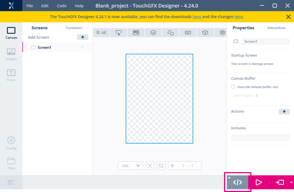
- 3. Click on the generate code icon on the bottom right corner.
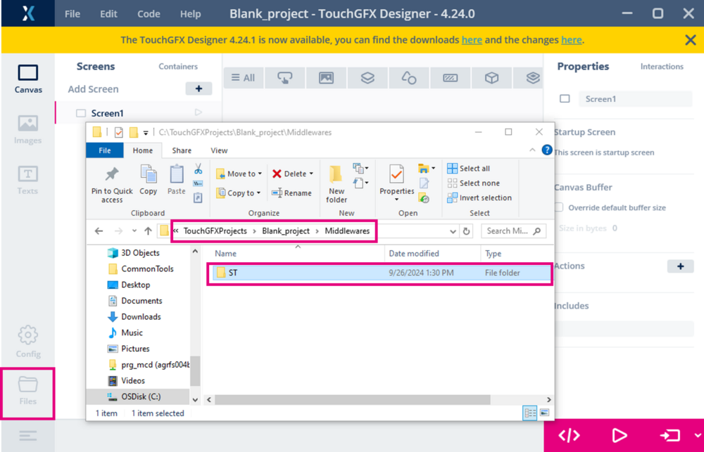
- 4. Click on the files icon on the bottom left corner, navigate to TouchGFXProjects/%Project_name%/Middlewares, and copy the ST folder.
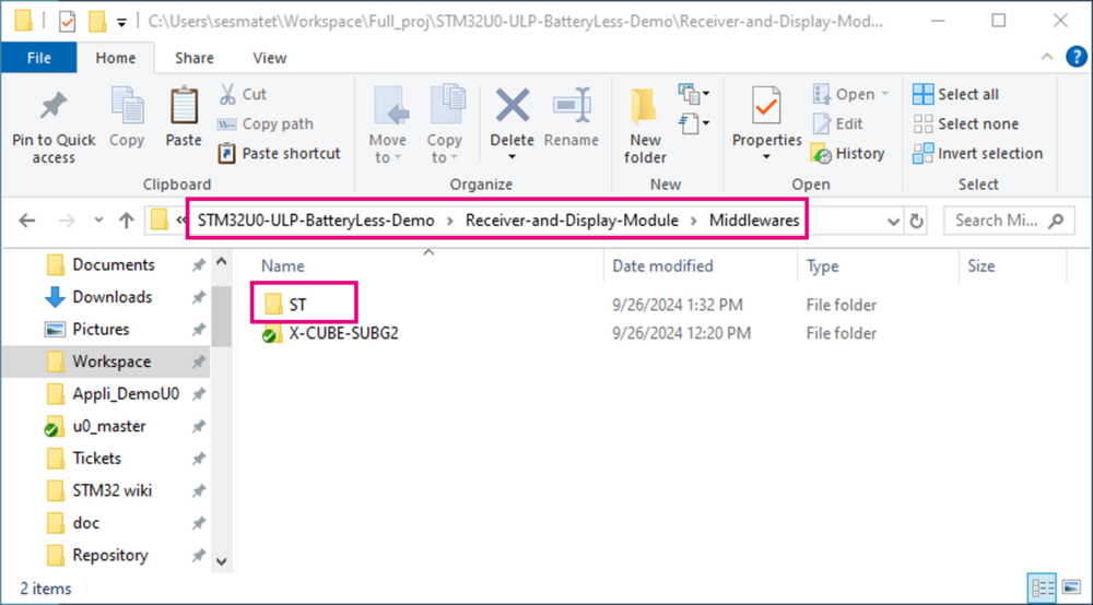
- 5. On the demo project folder, navigate to STM32U0-ULP-BatteryLess-Demo\Receiver-and-Display-Module\Middlewares and paste the folder here.
- 6. With IAR, Open the project.eww file located under STM32U0-ULP-BatteryLess-Demo\Receiver-and-Display-Module\EWARM.
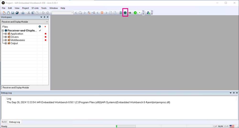
- 7. Build the project, by clicking on the make icon for example.
- 8. To flash the project, follow the steps of the Flashing directly with binary file section, but browse the “Reception_and_Display-Module.hex” file located STM32U0-ULP-BatteryLess-Demo\Receiver-and-Display-Module\EWARM\Receiver-and-Display-Module\Exe instead.
4. Behavior of the running demo
- Press the blue joystick button on the STM32U083C Discovery kit to switch between illuminance and temperature displayed on the LCD display.
- The data is sent only when the measured illuminance is over a defined threshold (150 lux in the original project). It is shown by the bars on the side on of the segment LCD display: if there is one bar going up, data is being sent - if the four bars are blinking, it means that no data is sent, to limit the energy used. The threshold can be changed in demo_config.h file, under the name THRESHOLD_LUX_NO_SENDING. In this file, other parameters can be changed to modify the configuration of the demo.
5. Known limitations
- As there is no unique identifier in the sending on the transmission side, the reception modules are plotting on the same graph from all transmission modules sending around.
- The data received can be out of range on the graph of the display. On the shared project that can be found on GitHub, it has been decided to show illuminance between 0 and 1000 lux, and temperatures between 16 and 36 degrees Celsius. Those values can be changed in the main.h file of the Receiver-and-Display-Module project. Those values have been chosen so it is possible to clearly see variations, especially for the illuminance graph.
6. References
- ↑ D6 and D7 connectors are used by the display module, so neither of them can be used for SDN pin.
- STM32U0 new product for entry level battery operated devices, video in which you can see running demo.
- STM32U0 ULP Lux demo, video presenting the principle of this demo.
- STM32U0 new product for entry level battery operated devices, video in which you can see running demo.

