This article explains what SPI is and uses examples to demonstrate how to use it.
1. What is Serial Peripheral Interface (SPI)?
Serial Peripheral Interface (SPI) is a synchronous serial communication interface specification used for short-distance communication, primarily in embedded systems. The interface was developed by Motorola in the mid-1980s and has become a de facto standard. SPI devices can communicate in full duplex mode using a master-slave architecture, with most often a single master. The master (controller) device originates the frame for reading and writing. Multiple slave devices may be supported through selection with individual chip select (CS), sometimes called slave select (SS), lines.
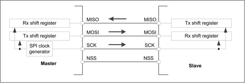
In full duplex mode with multiple slaves, SPI uses four buses:
- SCK (Serial Clock) bus, controlled by the master device
- MISO (Master Input Slave Output) bus
- MOSI (Master Output Slave Input) bus
- SS (Slave Select) bus, useful in the case of a multiple-slave configuration
1.1. STM32 SPI modes
The SPI interface is highly configurable, supports many standard protocols, and can operate in the following modes:
- Full duplex
- Half duplex
- Receive only
- Transmit only
1.2. STM32 SPI parameters
Basic parameters:
- Frame format: Motorola or TI
- Data size: 4 to 16 bits depending on STM32
- First bit: MSB or LSB
Clock parameters:
- Prescaler: from 2 to 256. Note that the SPI clock speed cannot exceed half the internal bus frequency.
- Clock polarity (CPOL): low or high
- Clock phase (CPHA): 1 or 2 edge
1.3. Main SPI HAL functions
Based on the STM32Cube HAL functions, SPI data transfer can be performed in three modes: blocking mode, interrupt mode, or DMA mode.
- Blocking mode:
- The communication is performed in polling mode. The status of all data processing is returned by the same function after finishing the transfer.
- HAL_SPI_Transmit()
- HAL_SPI_Receive()
- HAL_SPI_TransmitReceive()
- Non-blocking modes
- The communication is performed using interrupts or DMA. These functions return the status of the transfer startup.
- The end of the data processing is indicated through the dedicated SPI IRQ when using interrupt mode, or the DMA IRQ when using DMA mode.
- Interrupt mode:
- HAL_SPI_Transmit_IT()
- HAL_SPI_Receive_IT()
- HAL_SPI_TransmitReceive_IT()
- DMA mode:
- HAL_SPI_Transmit_DMA()
- HAL_SPI_Receive_DMA()
- HAL_SPI_TransmitReceive_DMA()
2. Configure the SPI to communicate between two boards
2.1. Objective
In this example, the objective is to set up communication between two NUCLEO-L476RG boards through SPI. Here, data is transmitted by the master device and received by the slave.
2.2. Master board project
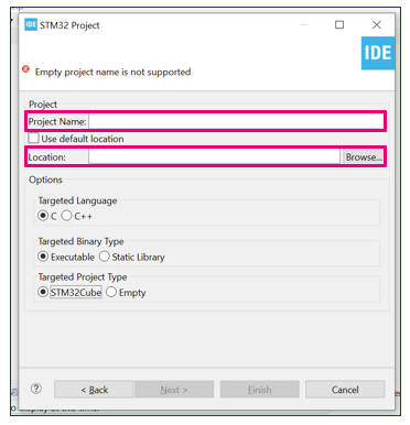
2.2.1. Create master project in STM32CubeIDE
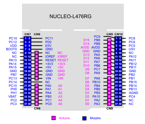
- The NUCLEO-L476RG pinout (illustrated by the figure below) is helpful to set the wiring between the boards in the project.
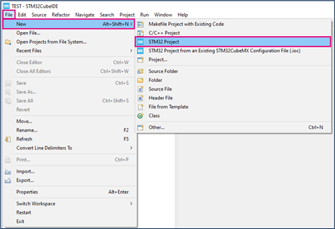
- Go to File>New>STM32 Project in the main window.
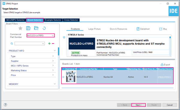
- Select the NUCLEO-L476RG board in the Board Selector tab as shown in the below figure.
If the STM32CubeL4 firmware package hasn't been downloaded yet, this will now start automatically (and may take some time).
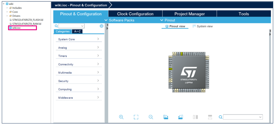
- Save the project.
2.2.2. Configure SPI on master board
- Open the STM32CubeMX project from the workspace.
2.2.2.1. SPI settings
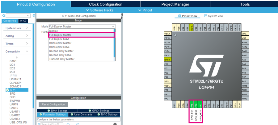
- Under Connectivity, select SPI1.
- Select Full-Duplex Master mode:
- Pin PA5 as SCK
- Pin PA6 as MISO
- Pin PA7 as MOSI
- Pin PA5 as SCK
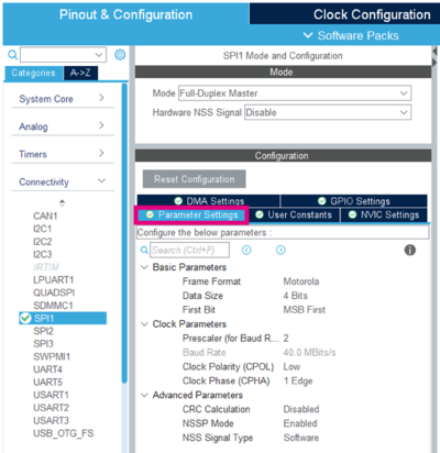
- Keep the default SPI settings, as shown below.
2.2.2.2. GPIO settings
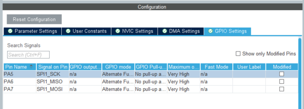
- Leave the GPIO settings in the default configuration, as shown below.
2.2.2.3. NVIC and DMA settings
- Interrupt mode only
- Go to the NVIC settings tab
- Enable SPI1 global interrupt
- Go to the NVIC settings tab
- DMA mode only
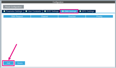
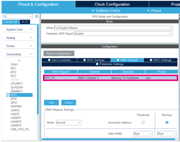
- Go to the DMA settings tab and click the Add button.
- Go to the DMA settings tab and click the Add button.
- Add SPI1_TX for the master board:
2.2.3. Generate source code and edit main.c
- Push "Ctrl+S" to generate the project and click "Yes" in the popup window, as shown below.
- Open main.c in the project explorer (/[myproject]/Src/main.c).
/* USER CODE BEGIN PV */
/* Private variables */
uint8_t TX_Buffer [] = "A" ; // DATA to send
/* USER CODE END PV */
- Blocking mode
/* USER CODE BEGIN 2 */
  HAL_SPI_Transmit(&hspi1, TX_Buffer, 1, 1000); //Sending in Blocking mode
  HAL_Delay(100);
/* USER CODE END 2 */
- Interrupt mode
/* USER CODE BEGIN 2 */
  HAL_SPI_Transmit_IT(&hspi1, TX_Buffer, 1); //Sending in Interrupt mode
  HAL_Delay(100);
/* USER CODE END 2 */
- DMA mode
/* USER CODE BEGIN 2 */
  HAL_SPI_Transmit_DMA(&hspi1, TX_Buffer, 1);; //Sending in DMA mode
  HAL_Delay(100);
/* USER CODE END 2 */
2.2.4. Compile project and program master board
- Click the Build button

- Click the Debug button (to run step by step)

- Or click the Run button (to execute)

2.3. Slave board project
2.3.1. Create slave project in STM32CubeIDE
- Create a new project, as described in #Create master project in STM32CubeIDE above.
2.3.2. Configure SPI on slave board
- Open the STM32CubeMX project from the workspace.
2.3.2.1. SPI settings
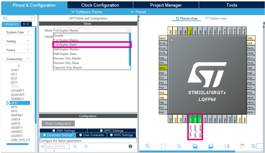
- Under Connectivity, select SPI1.
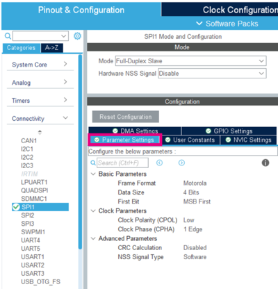
- Select Full-Duplex Slave mode:
- Pin PA5 as SCK
- Pin PA6 as MISO
- Pin PA7 as MOSI
- Pin PA5 as SCK
- Leave the SPI parameters settings in their default configuration, as shown below:
2.3.2.2. GPIO settings
- Keep the default GPIO settings, as shown below.
2.3.2.3. NVIC and DMA settings
- Interrupt mode only
- Go to the NVIC settings tab
- Enable SPI1 global interrupt
- Go to the NVIC settings tab
- DMA mode only
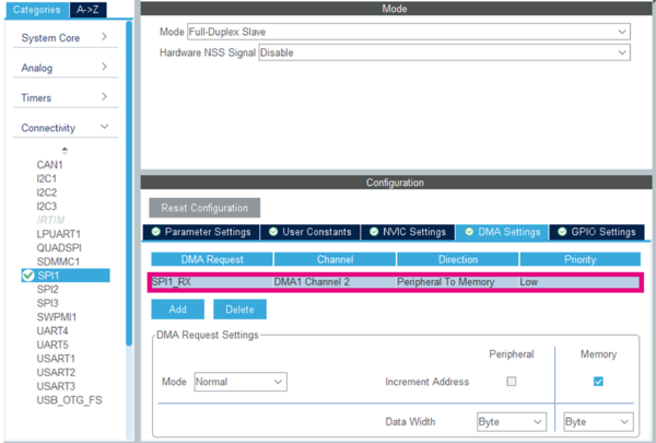
- Go to the DMA settings tab and click the Add button.
- Go to the DMA settings tab and click the Add button.
- Add SPI1_RX for the slave board:
2.3.3. Generate source code and edit main.c
- Push "Ctrl+S" to generate the project and click "Yes" in the popup window, as shown below.
- Open main.c in the project explorer (/[myproject]/Src/main.c).
/* USER CODE BEGIN PV */
/* Private variables */
uint8_t RX_Buffer [1] ; // DATA to receive
/* USER CODE END PV */
- Blocking mode
/* USER CODE BEGIN 2 */
  HAL_SPI_Receive(&hspi1, RX_Buffer, 1, 1000); //Receiving in Blocking mode
  HAL_Delay(100);
/* USER CODE END 2 */
- Interrupt mode
/* USER CODE BEGIN 2 */
  HAL_SPI_Receive_IT(&hspi1, RX_Buffer, 1); //Receiving in Interrupt mode
  HAL_Delay(100);
/* USER CODE END 2 */
- DMA mode
/* USER CODE BEGIN 2 */
  HAL_SPI_Receive_DMA(&hspi1, RX_Buffer, 1); //Receiving in DMA mode
  HAL_Delay(100);
/* USER CODE END 2 */
2.3.4. Compile and flash on slave board
- Click the Build button

- Click the Debug button (to run step by step)

- Or click the Run button (to execute)

2.4. Project workspace
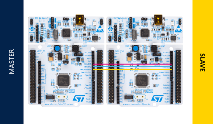
The following table shows the connection between two NUCLEO-L474RG boards using the SPI bus, requiring only three wires.
| NUCLEO-L476RG MASTER | NUCLEO-L476RG SLAVE | Pin description |
|---|---|---|
| PA5 | PA5 | SCK |
| PA6 | PA6 | MISO |
| PA7 | PA7 | MOSI |
