This article details an example of certification using Bluetooth® qualification workspace with STM32WBA55CG.
1. STM32WBA55CG reference PHY and stack QDIDs/DNs
Before going through this process, QDIDs/DNs used with STM32WBA55CG must be defined. The Bluetooth® Special Interest Group (SIG) provides a listing search [1] for finding previously qualified designs and declared products.
A dedicated certification guideline wiki page [2] provides the latest QDIDs/DNs to be used for each STM32WBAx product.
1.1. STM32WBA55CG reference RF-PHY
According to the dedicated certification guideline wiki page [2], DN Q320738 [3] should be considered.
This RF PHY was qualified with core specification 6.0 and using the test case reference list (TCRL) version 2024-2.
1.2. STM32WBA55CG reference stack
According to the dedicated certification guideline wiki page [2], DN Q330021 [4] should be considered.
These stacks were qualified with core specification 5.4 and using the test case reference list (TCRL) version 2023-1.
2. Qualification workspace process
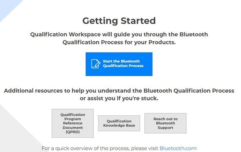
The Bluetooth® qualification workspace [5] is the starting point of certification journey.
Note that this page includes additional resources to help you understand the Bluetooth Qualification Process or assist you, in case of any issues.
To start, click on "Start the Bluetooth Qualification Process".
Each subchapter of this article describes a different step of the qualification process on the Bluetooth® website.
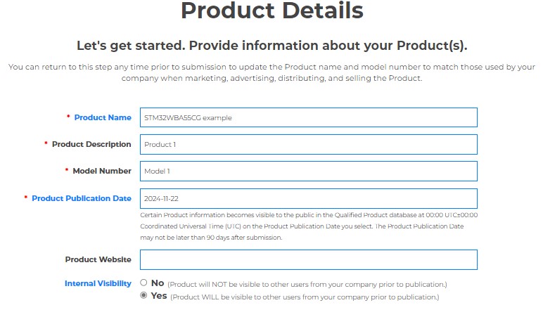
2.1. Product details
In this step, product details should be entered as illustrated in the following example.
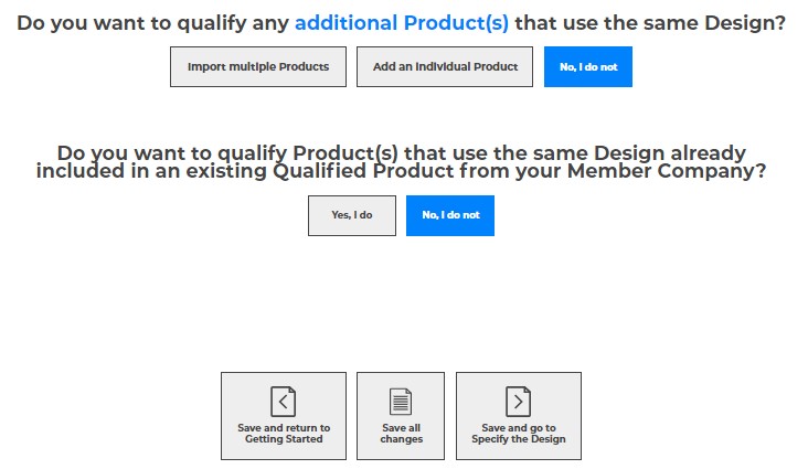
Once product details are entered, the customer can, if required, add an additional product. To move forward, "No, I do not" must be selected, as shown below.
2.2. Specify the design
Since the customer is reusing QDIDs/DNs, "Yes, I do" is selected, and both DNs associated with the STM32WBA55CG are entered, as shown below.
Once this is done, the following step must be completed:
The customer can now proceed to layer selection and select '"Save and go to the layer selection"
2.3. Layer selection
In this example, the customer is considering certifying a complete product with proprietary profile and should proceed as follows:
The customer can now proceed to ICS selection and select “Save and go to ICS selection”.
2.4. ICS selection
To avoid inconsistencies in the future, select "Core" and uncheck 1/60 as shown below.
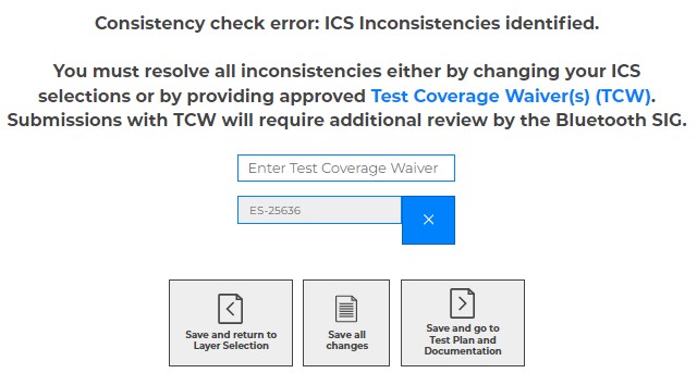
Then, the customer can confirm there are no inconsistencies by clicking the 'Consistency Check' button. As shown in the example below, many inconsistencies may appear.
Indeed, the ICS items mentioned do not exist in the layer. Consequently, the customer must use waiver TCW ES-25636 to resolve these inconsistencies. Note that this waiver is also mentioned in DN Q330021 [4].
At this stage, waiver must be added using ES-25636 waiver at bottom of ICS selection page as shown below.
The customer can proceed to the next step by selecting 'Save and go to Test plan and documentation'.
2.5. Test plan and documentation
In this example, no test plan should be generated for the new design thanks to the pre-qualified DNs associated to STM32WBA55.
However, some customers may have to select “Upload test declaration and test reports” and upload their own certified RF-PHY test report executed from certified test house (as explained in the dedicated Certification guideline wiki page [2]).
The customer can now complete the process with qualification fee payment.
2.6. Product Qualification Fee
In this step, product qualification fee needs to be addressed.
The customer can now complete the process with submission page.
2.7. Submission
The customer receives a summary of the requirements status based on the provided product declarations or reports.
Your qualification journey with STM32WBA55CG is now completed!
3. References


