Target description
This tutorial will help you to:
- Use the X-NUCLEO-SRC1M1 shield that includes a TCPP02-M18 protection circuit and provides a USB Type-C® connector
- Create a USB legacy 3A@5V Source application with the NUCLEO-F446RE board that does not include any UCPD peripheral and the X-NUCLEO-SRC1M1 shield by using STM32CubeIDE software
Prerequisites
- Computer with Windows 7 (or higher)
- Computer with Windows 7 (or higher)
Hardware
- NUCLEO-F446RE (tested on rev C-04) [1]
- X-NUCLEO-SRC1M1 shield [2]
- A USB-PD sink device to test our USB Source device (it can be the sink created in this wiki article, or a mobile phone or device)
- USB cable Type-A to Mini-B
- USB Type-C® to Type-C® cable
Software
Literature
Create a USB-PD Source Device
![]() Total 50min
Total 50min
1. Creating the project
![]() 5min
5min
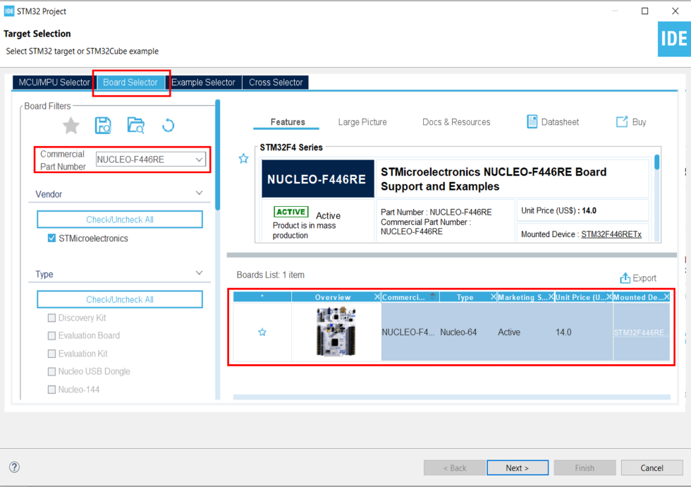
Open STM32CubeIDE and create a New STM32 Project. As a target selection, choose the NUCLEO-F446RE from the Board Selector Tab
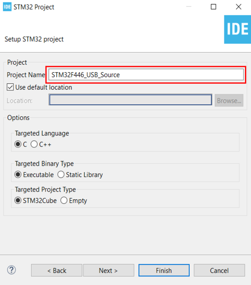
Click "Next", then enter your project's name. Leave the other fields as default and click "Finish".
When prompted for initializing peripherals with their default mode, click No.
2. Configuring the system
At this point, your project is created and you are left with the STM32CubeMX view.
In the next steps, we will configure the peripherals and options needed for the project.
2.1. Clear the pinout
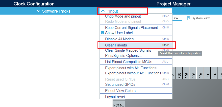
To start from a blank configuration, click on the Pinout menu and select Clear Pinouts. This will reset the pinouts in the Pinout view.
2.2. Configure the system timebase
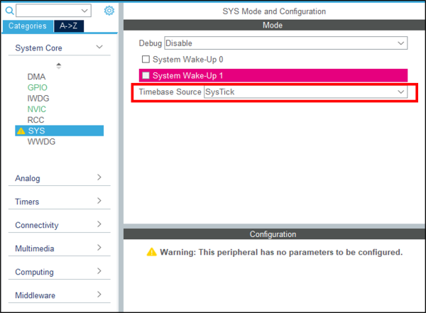
For this simple example, we will use SysTick as the system timebase. In the System Core section, select SYS and change the Timebase Source to SysTick.
2.3. Configure GPIO
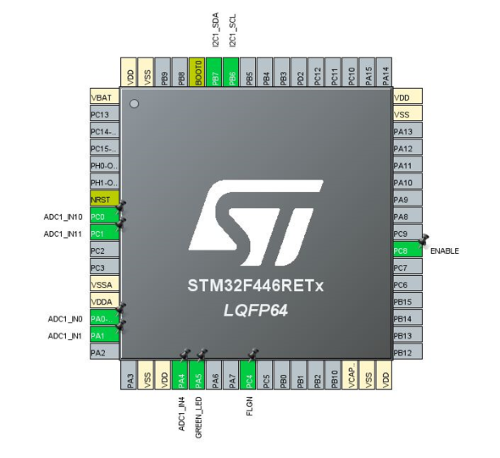
Three GPIO are used
- Click left on the pin PC8 and select GPIO_Output. With a right click select Enter user label to name it as ENABLE. This output will drive the TCPP02 chip enable input.
- Click left on the pin PA5 and select GPIO_Output. With a right click select Enter user label to name it as GREEN_LED. This output will drive the green led on the Nucleo board to indicate that Vbus is ON.
- Click left on the pin PA10 and select GPIO_EXT10, and with a right click select Enter user label to name it as 'FLGN'. This interrupt input will receive any TCPP02 fault flag.
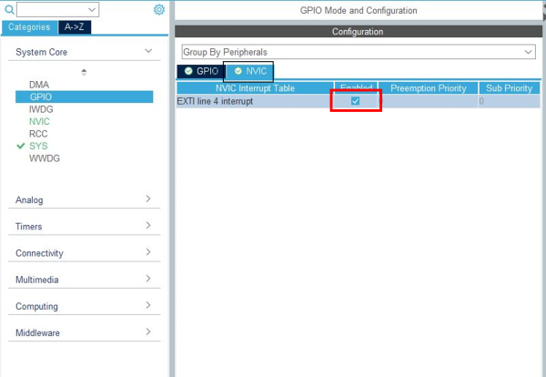
in the System Core section, select GPIO, and then change PA10 mode to "External interrupt Mode with Falling Edge detection".
Finally, in the NVIC tab, activate the EXTI lines[15-10] interrupts
2.4. Configure ADC peripheral
Five signals shall be monitored to ensure proper and safe USB 3A-5V delivery. CC1 and CC2 configurations lines voltage, Vbus and Vprovider voltages and Iana the current through Vbus. Then an ADC needs to be configured: In the pin view, with a left click, select the pin PC0, configure it as ADC1 Channel 10 (CC2). Repeat the operation for PC1 as ADC1 Channel 11 (IANA); for PA0 as ADC1 Channel 0 (VBusc); for PA1 as ADC1 Channel 1(Vprov); and for PA4 as ADC1 Channel 4 (CC1) Note: it is not mandatory to set their name as each value will be stored in a table by DMA in function of its rank.
2.4.1. ADC parameters configuration
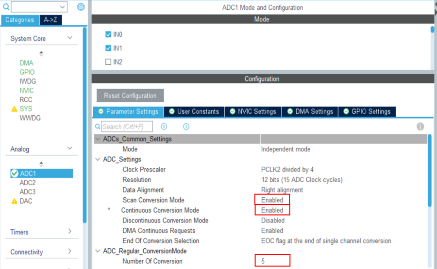
In the Analog section click on ADC and select, in the Parameter Settings tab:
- Scan conversion Mode: Enabled
- Continuous Conversion Mode: Enabled
- Number of conversions: 5
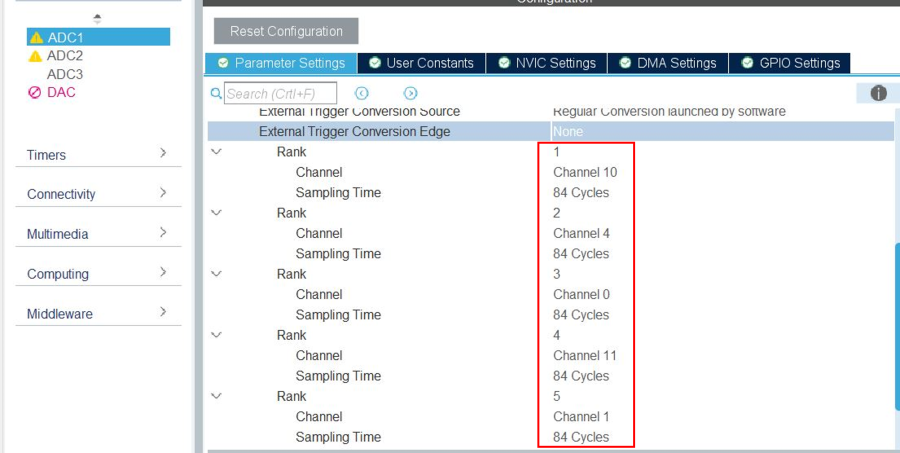
Then, define for each ADC input its channel and 144 Cycles Sampling time
- Rank 1: CC2: Channel 10
- Rank 2: CC1: Channel 4
- Rank 3: Vbus: Channel 0
- Rank 4: Iana: Channel 11
- Rank 5: Vprov: Channel 1
2.4.2. DMA Configuration for ADC1
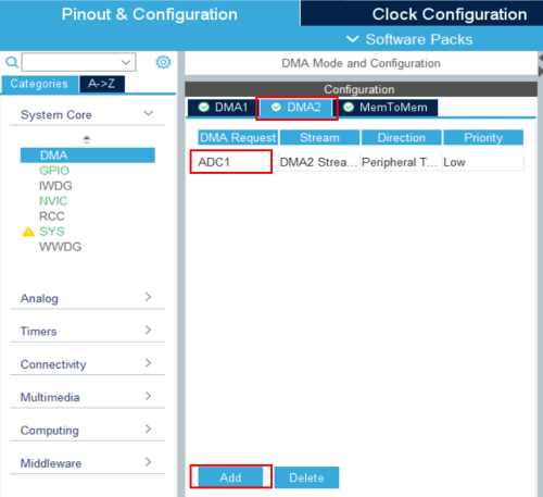
in the System Core section, select the DMA, tab DMA2 click on "ADD" and select ADC1 in the DMA2 request column.
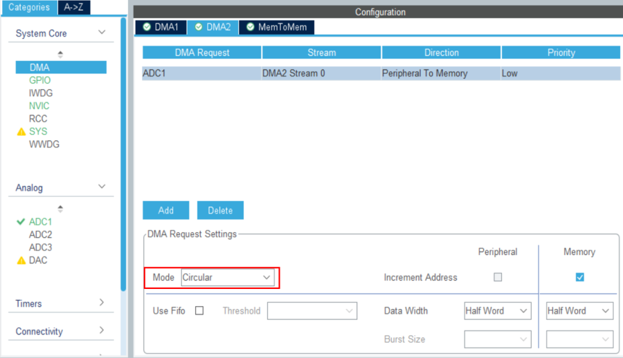
And set the DMA Mode: Circular
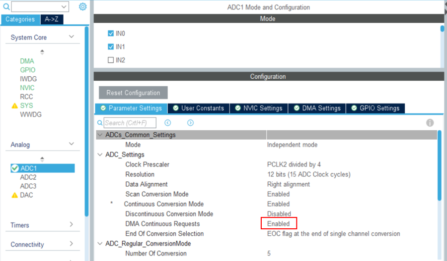
Then back to the ADC1 parameters configuration, set DMA Continuous Requests to Enabled
2.5. Configure TIM2 timer
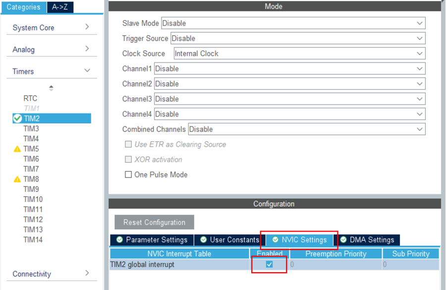
in the Timers section, select timer2: "TIM2", affect the "Internal clock" as clock source. In the Parameter Settings tab,
- Set the Prescaler value to 2000
- The counter period to 50
- The Internal clock division to "Division by 4"
Finally, select the NVIC Settings tab to enable the TIM2 global interrupt
2.6. Configure I2C peripheral
As the X-NUCLEO-SRC1M1 shield includes a TCPP02-M18 that communicates via I2C, we need to enable the I2C peripheral in our project.
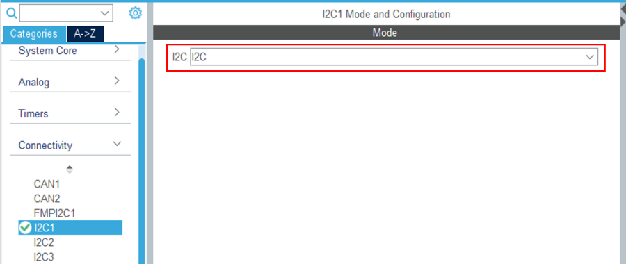
In the Connectivity section, enable I2C1 peripheral, in I2C mode. Leave the configuration as default, as the X-NUCLEO-SRC1M1 BSP will reconfigure it.
Note: We need to enable the I2C1 peripheral in the CubeMX view for code generation to include the I2C drivers.
2.7. Check the clock configuration
Under Clock Configuration main tab.
3. Configure project
![]() 5min
5min
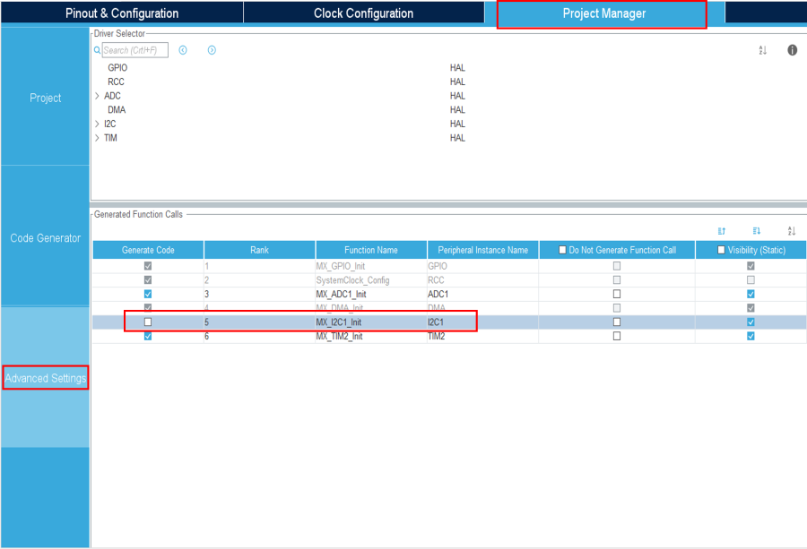
Under the Project Manager main tab, under the Advanced Settings tab, as we do not need I2C initialization functions (handled by the BSP drivers), uncheck Generate Code for the MX_I2C1_Init.
4. Add BSP to the project
![]() 5min
5min
Board Support Package (BSP) for the X-NUCLEO-SRC1M1 shield needs to be added to the project. The files need to be copied manually in the project's folder.
Get the latest BSP from GitHub x-cube-tcpp.
Manually copy the three following folders:
x-cube-tcpp
└── Drivers
    └── BSP
        ├── 📁X-NUCLEO-SRC1M1
        └── Components
            └── 📁tcpp0203
Into:
<ProjectFolder>
└── Drivers
    └── BSP
        ├── 📁X-NUCLEO-SRC1M1
        └── Components
            └── 📁tcpp0203
Then, create a file named ".extSettings" at the project's root folder (please mind the dot character in the filename) and fill it with the following code:
[ProjectFiles]
HeaderPath=Drivers\BSP\X-NUCLEO-SRC1M1;Drivers\BSP\Components\tcpp0203
[Others]
Define=TCPP0203_SUPPORT;USBPD_CONFIG_MX;USE_STM32F4XX_NUCLEO
HALModule=
[Groups]
Drivers/BSP/X-NUCLEO-SRC1M1=Drivers/BSP/X-NUCLEO-SRC1M1/src1m1_usbpd_pwr.c;Drivers/BSP/X-NUCLEO-SRC1M1/src1m1_bus.c
Drivers/BSP/Components/tcpp0203=Drivers/BSP/Components/tcpp0203/tcpp0203.c;Drivers/BSP/Components/tcpp0203/tcpp0203_reg.c
This file is used to tell the code generator to include the BSP files when generating the project.
5. Generate code
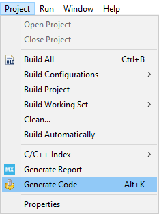
Save your file with Ctrl+s and select generate code if prompted. You can also generate code from the STM32CubeIDE menu by clicking Project/Generate Code, or by pressing Alt+K.
In this project, different folders can be found:
- The Core folder contains the source files for the core of the project.
- The Drivers folder contains the HAL drivers for the STM32, and the BSP for the Nucleo board and X-NUCLEO-SRC1M1 shield.
The Drivers folder in the Explorer view of the project must contain the BSP folders added earlier.
6. Complete application
![]() 15min
15min
Now that the peripherals are initialized by STM32CubeMX, some minimum level of the application needs to be added:
- src1m1_conf.h file needs to be created from its template, and added to the project
- User code needs to be added in several files
6.1. Add SRC1M1 configuration file
In the Drivers\BSP\X-NUCLEO-SRC1M1 folder you will find src1m1_conf_template.h. Copy it to Core\Inc folder, and rename it src1m1_conf.h. It is the configuration file used for the X-NUCLEO-SRC1M1 BSP.
6.2. Add code in main.h
Add the following code between the /* USER CODE BEGIN ET-END ET*/ tags:
/* USER CODE BEGIN ET */
typedef struct
{
    uint8_t Attaching_CC1;   /*Attachement on going - debouncing - Rp detected on CC1*/
    uint8_t Attaching_CC2;   /*Attachement on going - debouncing - Rp detected on CC2*/
    uint8_t Attached_CC1;    /*Attached - Rp on CC1*/
    uint8_t Attached_CC2;    /*Attached - Rp on CC2*/
    uint8_t Detaching;       /*Detachement on going*/
    uint8_t Discharging;     /*Vbus is discharging on going*/
    uint8_t TCPP_Fault;	     /*Hardware detected fault (Isense)*/
}USB_C_Typedef;
/* USER CODE END ET */
Add the following code between the /* USER CODE BEGIN EC-END EC*/ tags:
/* USER CODE BEGIN EC */
/* USB PWR ADC Index */
#define ADC_CC1_Index                              0   /* CC1 index in adc value table */
#define ADC_CC2_Index                              1   /* CC2 index in adc value table */
#define ADC_VBUSC_Index                            2   /* VBus index in adc value table */
#define ADC_ISENSE_Index                           3   /* Isense index in adc value table */
#define ADC_VPROV_Index                            4   /* Vprov index in adc value table */
/* USB PWR ADC Applicatives Limits */
#define USBnoPD_CC_Voltage_MaxRa                   800  /* CC line Max voltage when Ra is connected (in mV) */
#define USBnoPD_CC_Voltage_MinRd                   850  /* CC line Min voltage when connected to Rd (in mV) */
#define USBnoPD_CC_Voltage_MaxRd                   2450 /* CC line Max voltage when connected to Rd (in mV) */
#define USBnoPD_CC_Voltage_MinOpen                 2750 /* CC line Minimum voltage when not connected (in mV) */
#define USBnoPD_VBUS_Voltage_Max                   5500 /* Vbus Maximum allowed voltage (in mV) */
#define USBnoPD_VPROV_Voltage_Min                  1000 /* Vprov Minimum voltage (in mV) */
#define USBnoPD_VSAFE_Voltage_Max                  80   /* Vbus safe voltage to end vbus discharge (in mV) */
#define USBnoPD_ISENSE_Max                         1900 /* decimal for 4A */
/* USER CODE END EC */
6.3. Add code in main.c
Add the following code between the /*USER CODE BEGIN Includes-END Includes*/ tags:
/* USER CODE BEGIN Includes */
#include "src1m1_usbpd_pwr.h"
/* USER CODE END Includes */
Add the following code between the /*USER CODE BEGIN PV-END PV*/ tags :
/* USER CODE BEGIN PV */
  uint16_t value_adc[5];
  uint16_t value_adc_filtered[5]={0,0,0,0,0};
  USB_C_Typedef USB_C;
/* USER CODE END PV */
Add the following code between the /*USER CODE BEGIN 2-END 2*/ tags :
  /* USER CODE BEGIN 2 */
  HAL_GPIO_WritePin(GREEN_LED_GPIO_Port,GREEN_LED_Pin,GPIO_PIN_RESET);
  HAL_GPIO_WritePin(ENABLE_GPIO_Port,ENABLE_Pin,GPIO_PIN_SET);

  BSP_USBPD_PWR_Init(0);
  BSP_USBPD_PWR_SetPowerMode(0,USBPD_PWR_MODE_NORMAL);

  USB_C.Attaching_CC1=0;
  USB_C.Attaching_CC2=0;
  USB_C.Attached_CC1=0;
  USB_C.Attached_CC2=0;
  USB_C.Detaching=0;
  USB_C.Discharging=0;
  USB_C.TCPP_Fault=0;

  HAL_ADC_Start_DMA(&hadc1,(uint32_t*)&value_adc,5);
  /* USER CODE END 2 */
6.4. Modification in stm32f4xx_it.c
Add the following code between the /* USER CODE BEGIN-END Includes */ tags:
/* USER CODE BEGIN Includes */
#include "src1m1_usbpd_pwr.h"
/* USER CODE END Includes */
Add the following code between the /*USER CODE BEGIN-END PFP * tags:
/* USER CODE BEGIN PFP */
static uint32_t USBnoPD_TCPP0203_ConvertADCDataToVoltage(uint32_t ADCData, uint32_t Ra, uint32_t Rb);
/* USER CODE END PFP */
Add the following code between the /*USER CODE BEGIN-END EV * tags:
/* USER CODE BEGIN EV */
  extern USB_C_Typedef USB_C;
  extern uint16_t value_adc[];
  extern uint16_t value_adc_filtered[];
/* USER CODE END EV */
In the TIM2 IRQ Handler, add the following code between the /*USE CODE BEGIN TIM2_IRQn 0-END TIM2_IRQn 0*/ tags:
  /* USER CODE BEGIN TIM2_IRQn 0 */
  if (USB_C.Attaching_CC1>=1)
  {
    USB_C.Attaching_CC1++;
  }
  if (USB_C.Attaching_CC2>=1)
  {
    USB_C.Attaching_CC2++;
  }
  if (USB_C.Detaching)
  {
	USB_C.Detaching++;
  }
  __HAL_TIM_SET_COUNTER(&htim2, 0);
  /* USER CODE END TIM2_IRQn 0 */
In the EXTI10-15 IRQ Handler, add the following code between the /*USE CODE BEGIN EXTI10_IRQn 0-END EXTI10_IRQn 0*/ tags:
  /* USER CODE BEGIN EXTI10_IRQn 0 */
  //TCPP FLGn flag Active low
  USB_C.Discharging=1;
  BSP_USBPD_PWR_VBUSOff(0);
  BSP_USBPD_PWR_VBUSDischargeOn(0);
  HAL_GPIO_WritePin(GREEN_LED_GPIO_Port,GREEN_LED_Pin,GPIO_PIN_RESET);
  if (USB_C.Attached_CC1==1)
  {
    USB_C.TCPP_Fault=1;
  }
  if (USB_C.Attached_CC2==1)
  {
    USB_C.TCPP_Fault=2;
  }
  /* USER CODE END EXTI10_IRQn 0 */
  HAL_GPIO_EXTI_IRQHandler(GPIO_PIN_10);
  /* USER CODE BEGIN EXTI15_10_IRQn 1 */
In the DMA2 IRQ Handler, add the following code between the /*USE CODE BEGIN DMA2_Stream0_IRQn 0-END DMA2_Stream0_IRQn 0*/ tags:
  /* USER CODE BEGIN DMA2_Stream0_IRQn 0 */
  /*Filtering ADC*/
  uint8_t i;
  for (i=0;i<5;i++)
  {
    value_adc_filtered[i]=(value_adc_filtered[i]+value_adc[i])/2;
  }
  /*Connection detection*/
  if ((USB_C.Attached_CC1==0)&&(USB_C.Attached_CC2==0)&&(USB_C.TCPP_Fault==0)&&
     (USBnoPD_TCPP0203_ConvertADCDataToVoltage(value_adc_filtered[ADC_VPROV_Index],SRC1M1_VSENSE_RA,SRC1M1_VSENSE_RB)>USBnoPD_VPROV_Voltage_Min))  /* No fault, No connection, Vbus=Vsafe0 */
  {
    if (((USBnoPD_TCPP0203_ConvertADCDataToVoltage(value_adc_filtered[ADC_CC1_Index],SRC1M1_NORA,SRC1M1_NORB)>USBnoPD_CC_Voltage_MinRd)&&
       ((USBnoPD_TCPP0203_ConvertADCDataToVoltage(value_adc_filtered[ADC_CC1_Index],SRC1M1_NORA,SRC1M1_NORB)<USBnoPD_CC_Voltage_MaxRd))&&
       ((USBnoPD_TCPP0203_ConvertADCDataToVoltage(value_adc_filtered[ADC_CC2_Index],SRC1M1_NORA,SRC1M1_NORB)<USBnoPD_CC_Voltage_MaxRa)|
       (USBnoPD_TCPP0203_ConvertADCDataToVoltage(value_adc_filtered[ADC_CC2_Index],SRC1M1_NORA,SRC1M1_NORB)>USBnoPD_CC_Voltage_MinOpen))))
    {
      if (USB_C.Attaching_CC1==0)
      {
        USB_C.Attaching_CC1=1;
        HAL_TIM_Base_Start_IT(&htim2);
      }
      if (USB_C.Attaching_CC1>=110)
      {
        HAL_TIM_Base_Stop_IT(&htim2);
        BSP_USBPD_PWR_VBUSDischargeOff(0);
        BSP_USBPD_PWR_VBUSOn(0);														/*TCPP Vbus MOS ON*/
        USB_C.Attaching_CC1=0;
        USB_C.Attaching_CC2=0;
        USB_C.Attached_CC1=1;
	    USB_C.Attached_CC2=0;
	    USB_C.Detaching=0;
        HAL_GPIO_WritePin(GREEN_LED_GPIO_Port,GREEN_LED_Pin,GPIO_PIN_SET);
      }
    }
    else if (((USBnoPD_TCPP0203_ConvertADCDataToVoltage(value_adc_filtered[ADC_CC2_Index],SRC1M1_NORA,SRC1M1_NORB)>USBnoPD_CC_Voltage_MinRd)&&
            ((USBnoPD_TCPP0203_ConvertADCDataToVoltage(value_adc_filtered[ADC_CC2_Index],SRC1M1_NORA,SRC1M1_NORB)<USBnoPD_CC_Voltage_MaxRd))&&
            ((USBnoPD_TCPP0203_ConvertADCDataToVoltage(value_adc_filtered[ADC_CC1_Index],SRC1M1_NORA,SRC1M1_NORB)<USBnoPD_CC_Voltage_MaxRa)|
            (USBnoPD_TCPP0203_ConvertADCDataToVoltage(value_adc_filtered[ADC_CC1_Index],SRC1M1_NORA,SRC1M1_NORB)>USBnoPD_CC_Voltage_MinOpen))))
    {
	  if (USB_C.Attaching_CC2==0)
      {
	    USB_C.Attaching_CC2=1;
		HAL_TIM_Base_Start_IT(&htim2);
	  }
	  if (USB_C.Attaching_CC2>=110)
      {
	    HAL_TIM_Base_Stop_IT(&htim2);
        BSP_USBPD_PWR_VBUSDischargeOff(0);
        BSP_USBPD_PWR_VBUSOn(0);														/*TCPP Vbus MOS ON*/
        USB_C.Attaching_CC1=0;
        USB_C.Attaching_CC2=0;
        USB_C.Attached_CC1=0;
        USB_C.Attached_CC2=1;
        USB_C.Detaching=0;
        HAL_GPIO_WritePin(GREEN_LED_GPIO_Port,GREEN_LED_Pin,GPIO_PIN_SET);
      }
    }
  }
  /*debouncing connection CC1*/
  if ((USB_C.Attaching_CC1>=1)&&(USBnoPD_TCPP0203_ConvertADCDataToVoltage(value_adc_filtered[ADC_CC1_Index],SRC1M1_NORA,SRC1M1_NORB)>USBnoPD_CC_Voltage_MaxRd))
  {
    USB_C.Attaching_CC1=0;																	/*If glitch detected : time restarts at beginning*/
  }
  /*debouncing connection CC2*/
  if ((USB_C.Attaching_CC2>=1)&&(USBnoPD_TCPP0203_ConvertADCDataToVoltage(value_adc_filtered[ADC_CC2_Index],SRC1M1_NORA,SRC1M1_NORB)>USBnoPD_CC_Voltage_MaxRd))
  {
    USB_C.Attaching_CC2=0;																	/*If glitch detected : time restarts at beginning*/
  }

  /*----------------------------------------------------------------*/
  /*Disconnection detection*/
  if (((USB_C.Attached_CC1==1)&&(USBnoPD_TCPP0203_ConvertADCDataToVoltage(value_adc_filtered[ADC_CC1_Index],SRC1M1_NORA,SRC1M1_NORB)>USBnoPD_CC_Voltage_MaxRd))|
     ((USB_C.Attached_CC2==1)&&(USBnoPD_TCPP0203_ConvertADCDataToVoltage(value_adc_filtered[ADC_CC2_Index],SRC1M1_NORA,SRC1M1_NORB)>USBnoPD_CC_Voltage_MaxRd)))
  {
    if (USB_C.Detaching==0)
    {
      USB_C.Detaching=1;
      HAL_TIM_Base_Start_IT(&htim2);
    }
    if (USB_C.Detaching>=10)
    {
      USB_C.Attached_CC1=0;
      USB_C.Attached_CC2=0;
      USB_C.Discharging=1;
      USB_C.Detaching=0;
      BSP_USBPD_PWR_VBUSOff(0);
      BSP_USBPD_PWR_VBUSDischargeOn(0);
      HAL_GPIO_WritePin(GREEN_LED_GPIO_Port,GREEN_LED_Pin,GPIO_PIN_RESET);
    }
  }
  if (((USB_C.Attached_CC1==1)&&(USBnoPD_TCPP0203_ConvertADCDataToVoltage(value_adc_filtered[ADC_CC1_Index],SRC1M1_NORA,SRC1M1_NORB)<USBnoPD_CC_Voltage_MaxRd))|
     ((USB_C.Attached_CC2==1)&&(USBnoPD_TCPP0203_ConvertADCDataToVoltage(value_adc_filtered[ADC_CC2_Index],SRC1M1_NORA,SRC1M1_NORB)<USBnoPD_CC_Voltage_MaxRd)))
  {
    USB_C.Detaching=0;
  }

  /*-----------------------------------------------------------------*/
  /* Fault Vbus too high or I too high */
  if (((USB_C.Discharging==0)&&(USB_C.TCPP_Fault==0))&&((USBnoPD_TCPP0203_ConvertADCDataToVoltage(value_adc_filtered[ADC_VBUSC_Index],SRC1M1_VSENSE_RA,SRC1M1_VSENSE_RB)>USBnoPD_VBUS_Voltage_Max)|
     (USBnoPD_TCPP0203_ConvertADCDataToVoltage(value_adc_filtered[ADC_VPROV_Index],SRC1M1_VSENSE_RA,SRC1M1_VSENSE_RB)<USBnoPD_VPROV_Voltage_Min)))
  {
    if (USB_C.Attached_CC1==1)
    {
      USB_C.Discharging=1;
      USB_C.Detaching=0;
      USB_C.TCPP_Fault=1;
      BSP_USBPD_PWR_VBUSOff(0);															/*Open MOS*/
      BSP_USBPD_PWR_VBUSDischargeOn(0);													/*Close Vbus discharge path*/
      HAL_GPIO_WritePin(GREEN_LED_GPIO_Port,GREEN_LED_Pin,GPIO_PIN_RESET);
    }
    if (USB_C.Attached_CC2==1)
    {
      USB_C.Discharging=1;
      USB_C.Detaching=0;
      USB_C.TCPP_Fault=2;
      BSP_USBPD_PWR_VBUSOff(0);															/*Open MOS*/
      BSP_USBPD_PWR_VBUSDischargeOn(0);													/*Close Vbus discharge path*/
      HAL_GPIO_WritePin(GREEN_LED_GPIO_Port,GREEN_LED_Pin,GPIO_PIN_RESET);
    }
  }

  /*-------------------------------------------------------------------*/
  /*End of Vbus discharge -> TCPP in Low Power*/
  if (USB_C.Discharging==1)		//If Vbus discharge was Requested
  {
    if (USBnoPD_TCPP0203_ConvertADCDataToVoltage(value_adc_filtered[ADC_VBUSC_Index],SRC1M1_VSENSE_RA,SRC1M1_VSENSE_RB)<USBnoPD_VSAFE_Voltage_Max)	/*Vbus is 0*/
    {
      USB_C.Discharging=0;
      USB_C.Detaching=0;
      BSP_USBPD_PWR_VBUSDischargeOff(0);
      HAL_GPIO_WritePin(GREEN_LED_GPIO_Port,GREEN_LED_Pin,GPIO_PIN_RESET);
    }
  }
  if (((USB_C.TCPP_Fault==1)&&(USBnoPD_TCPP0203_ConvertADCDataToVoltage(value_adc_filtered[ADC_CC1_Index],SRC1M1_NORA,SRC1M1_NORB)>USBnoPD_CC_Voltage_MinOpen))|
     ((USB_C.TCPP_Fault==2)&&(USBnoPD_TCPP0203_ConvertADCDataToVoltage(value_adc_filtered[ADC_CC2_Index],SRC1M1_NORA,SRC1M1_NORB)>USBnoPD_CC_Voltage_MinOpen)))
  {
    USB_C.Attached_CC1=0;
    USB_C.Attached_CC2=0;
    USB_C.Detaching=0;
    USB_C.TCPP_Fault=0;
    HAL_GPIO_WritePin(GREEN_LED_GPIO_Port,GREEN_LED_Pin,GPIO_PIN_RESET);
  }
  /*-------------------------------------------------------------------*/

  /* USER CODE END DMA2_Stream0_IRQn 0 */
Add the following code between the /* USER CODE BEGIN-END 1 */ tags:
/* USER CODE BEGIN 1 */
static uint32_t USBnoPD_TCPP0203_ConvertADCDataToVoltage(uint32_t ADCData, uint32_t Ra, uint32_t Rb)
{
  uint32_t VDD = 3300U;
  uint32_t ADC_MAX =  0x0FFF;
  uint32_t voltage;
  uint32_t vadc;

  vadc = (ADCData * VDD) / ADC_MAX;

  if ((Ra == 0u) && (Rb == 0u))
  {
    voltage = vadc;
  }
  else
  {
    voltage = vadc * (Ra + Rb) / Rb;
  }

  return voltage;
}
/* USER CODE END 1 */
7. Configure the shield's jumpers
Place jumpers on the X-NUCLEO-SRC1M1 shield as shown in the picture.
Next, plug an external 5V source into the green "source" connector.
With this configuration, the board will be powered by the ST-Link of the Nucleo board.
If you want to power your system from the external power supply connected to the "source" terminal, and not from the ST-Link, please add the JP1 jumpers between 1-2 and 3-4.
To increase the solution current capability to 3A @ 5V,
- Remove R35 and place it on SH19
- Remove R39 and place it on SH21
- Replace R4 sense resistor (initially 7mOhms) with a 10mOhms resistor
8. Compile and run the application
The compilation must be performed without error or warnings.
Build the application by clicking on the ![]() button (or select Project/Build Project).
button (or select Project/Build Project).
Run the application by clicking on the ![]() button (or select Run/Run)
button (or select Run/Run)
9. Evaluate the application
![]() 5min
5min
Vbus is active 120ms after plugging an USB Type-C source device.
Vbus is immediately shutdown and placed in safe mode (0V) when unplugging the sink device.
During connection, if an overcurrent or malfunction is detected, the Source is placed in safe mode (0V) and needs a disconnection/reconnection to restart.
You can find other applicative examples on GitHub: x-cube-tcpp
10. References
[[Category:STM32 step by step advance|30]]
[[Category:USB Power Delivery|20]]
