Template:ArticleMainWriter Template:ArticleApprovedVersion
1. ROM Code overview[edit source]
ROM code is the first code executed after a reset.
1.1. ROM code features[edit source]
- The main features of ROM code include:
- Secure Boot from serial link (Serial boot)
- Secure Boot from various Flash memories (Flash memory boot)
- Engineering boot
- RMA boot
- Wake up from low power modes
- Exported secure services
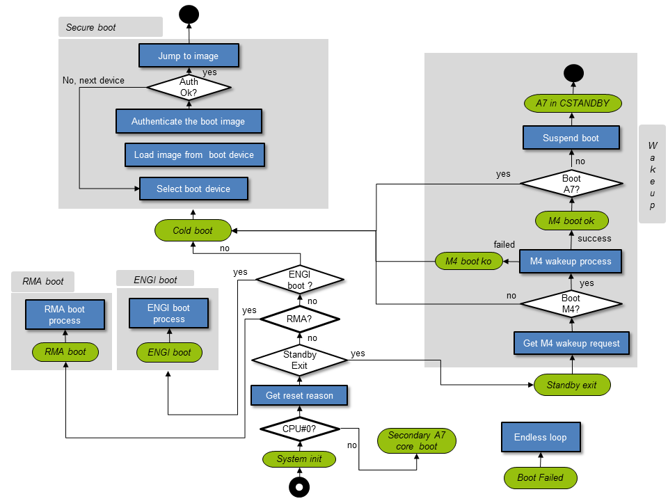
1.2. Device states[edit source]
The ROM code behaviour is strongly linked to the device state.
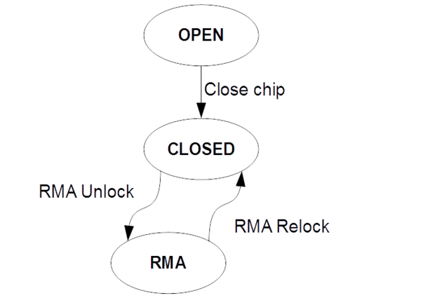
- Open state: By default the device is in open state. Authentication is not mandatory. An authentication error does not prevent FSBL from beeing started.
- Closed state: The device can be closed by writing to bit 6 of OTP WORD0. On closed devices, authentication is mandatory. An authentication error prevents FSBL from beeing started.
- RMA state: A closed device can be put once in RMA state and back again in closed state. On devices in RMA state, all ROM code features, except the one used to go back in closed state are disabled.
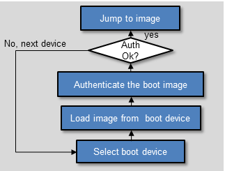
2. Secure boot[edit source]
The ROM code ensures the first stage of the STM32MP15 secure boot, implemented in the trusted boot chain:
- it loads FSBL image from selected boot interface
- it authenticates FSBL image
- if image is authenticated, it jumps to FSBL image entry point
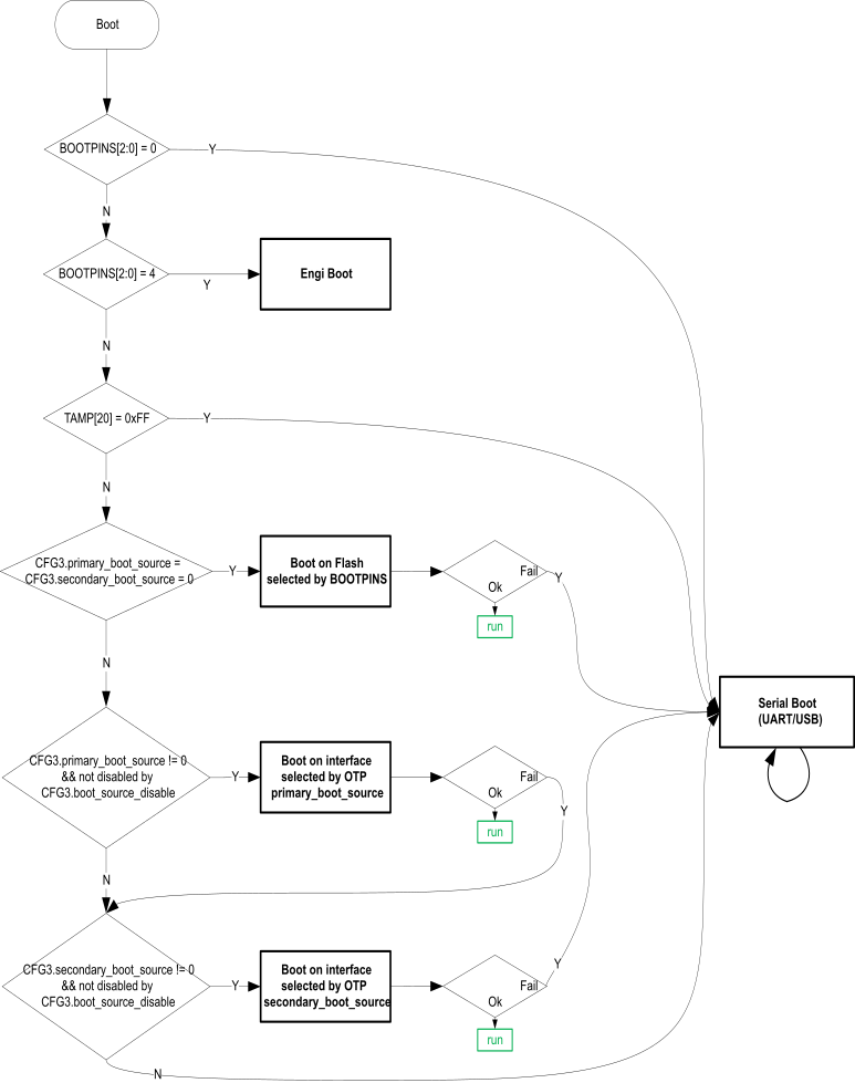
2.1. Boot interface selection[edit source]
As shown in the figure below, the boot interface is determined by the configuration given by boot pins, OTP and a TAMP register.
2.2. Image loading[edit source]
The ROM code loads the image into SYSRAM internal memory at address 0x2ffc2400.
2.3. FSBL authentication[edit source]
ROM code implements authentication process as described in STM32MP15 secure boot, Authentication processing chapter.
2.4. Jump to FSBL[edit source]
If image authentication is successful, the ROM code stores the address of the boot context in r0 register and jumps to the FSBL entry point defined in image header.
The boot context (see boot_api_context_t structure in plat/st/stm32mp1/include/boot_api.h ) is in the first 512 bytes of SYSRAM. It contains information on boot process (such as the selected boot device) and pointers to the ROM code services (used for secure boot authentication).
3. Serial boot[edit source]
The ROM supports UART and USB serial interfaces.
When serial boot is selected, the ROM code scans in parallel all bootable UART instances and the USB OTG. When an activity is detected on an interface, the boot process goes on with this interface and the others are ignored.
3.1. USB Boot[edit source]
The ROM supports boot on USB OTG interface with HS PHY.
USB OTG HS is clocked by a 48 MHz and a 60 MHz clock, generated by using HSE clock (from RCC).
The ROM code supports following HSE values:
8, 10, 12, 14, 16, 20, 24, 25, 26, 28, 32, 36, 40, 48 MHz
The ROM code selects which HSE it must use by following these steps:
- If OTP WORD 3.HSE_value is 0b00 (default behaviour), then the ROM code autodetects HSE by using HSI clock (from RCC).
- Recognized values are either 8, 10, 12, 14, 16, 20, 24, 32, 36, 28, 40, or 48 MHz.
- If none of these value can be recognized, the ROM code considers that HSE = 24 MHz.
- If OTP WORD 3.HSE_value is 0b01, then it considers that HSE=24 MHz
- If OTP WORD 3.HSE_value is 0b10, then it considers that HSE=25 MHz
- If OTP WORD 3.HSE_value is 0b11, then it considers that HSE=26 MHz
3.2. UART Boot[edit source]
The ROM supports the following UART interfaces:
- USART/UART instances:
- USART2, USART3, UART4, UART5, USART6, UART7, UART8
- (one start bit, 8 data bits, even parity bit and one stop bit).
Configuration:
By default the ROM code scans all UARTs listed above. This list may be reduced by blowing fuses in uart_intances_disable field of OTP WORD 3.
In case of Serial boot, the ROM code applies the following AFmuxes.
The ROM code first muxes only the RX pins of bootable UART instances and scans in parallel all these RX lines. When an activity is detected on an UART interface, the ROM code muxes the related TX, all others RX are unmuxed, and the boot process goes on with this interface.
In case of USB boot detection, all UART RX are unmuxed.
| UARTs | ||||||||||||||||||||||||||||||||||||||||||||||||||||||||||
|---|---|---|---|---|---|---|---|---|---|---|---|---|---|---|---|---|---|---|---|---|---|---|---|---|---|---|---|---|---|---|---|---|---|---|---|---|---|---|---|---|---|---|---|---|---|---|---|---|---|---|---|---|---|---|---|---|---|---|
|
|
| ||||||||||||||||||||||||||||||||||||||||||||||||||||||||
4. Flash memory boot[edit source]
The ROM supports the following Flash interfaces:
- QSPI NOR Flash via QUADSPI internal peripheral
- QSPI NAND Flash via QUADSPI internal peripheral
- FMC NAND Flash via FMC internal peripheral
- SD card via SDMMC internal peripheral
- e•MMC™ via SDMMC internal peripheral
Please refer to STM32MP15 Flash mapping article to see the details about the mapping of each of these memories.
4.1. Boot from NAND[edit source]
NAND contains n copies of FSBL in n first blocks. The ROM code scans blocks from the first and loads the FSBL contained in the first valid block.
The ROM code supports FMC (parallel) NANDs and QSPI (serial) NANDs.
Supported FMC (parallel) NANDs:
The ROM code supports FMC NAND with the following parameters.
| Block size (KBytes ) |
Page size (KBytes) |
Data width | ECC1(bits and code) |
|---|---|---|---|
| 128 | 2 | 8, 16 | 4 (bch), 8 (bch), 1 (hamming) |
| 256 | 4 | 8, 16 | 4 (bch), 8 (bch), 1 (hamming) |
| 512 | 4 | 8, 16 | 4 (bch), 8 (bch), 1 (hamming) |
| 512 | 8 | 8, 16 | 4 (bch), 8 (bch), 1 (hamming) |
- 1: The ROM code supports both FMC NAND with or without on-die ECC. The ECC given here is for NAND without on-die ECC.
Supported QSPI (serial) NANDs:
The ROM code supports QSPI NAND with the following parameters.
| Block size (KBytes) |
Page size (KBytes) |
|---|---|
| 128 | 2 |
| 256 | 4 |
| 512 | 4 |
| 512 | 8 |
Configuration:
In order to read a NAND flash, the ROM code needs to know the page size, the block size and the number of blocks. For FMC NAND it also needs to know the width and the number of ECC bits.
The ROM code detects NAND parameters storage location by checking OTP WORD9.nand_param_stored_in_otp value.
If OTP WORD9.nand_param_stored_in_otp value is equal to 0 (which is the default) then the NAND shall provide an ONFI compliant parameter table in which the ROM code looks for NAND parameters. “ONFI compliant” means that a NAND provides an ONFI get parameter command that returns a table where at least parameters needed by ROM code are located at standard ONFI offsets.
If OTP WORD9.nand_param_stored_in_otp value is equal to 1, the ROM code looks for NAND parameters in OTP WORD9.
The number of ECC bits is a particular case, as it can be set by OTP even if OTP WORD9.nand_param_stored_in_otp is equal to 0. This is to allow the user to override the recommanded number of ECC bits given by the parameter table of an ONFI NAND.
In case of QSPI NAND boot, the ROM code applies the same AFmuxes as the ones for QSPI NOR.
In case of FMC NAND boot, the ROM code applies the following AFmuxes:
| FMC NAND | |||||||||||||||||||||||||||||||||||||||||||||||||||||
|---|---|---|---|---|---|---|---|---|---|---|---|---|---|---|---|---|---|---|---|---|---|---|---|---|---|---|---|---|---|---|---|---|---|---|---|---|---|---|---|---|---|---|---|---|---|---|---|---|---|---|---|---|---|
|
| ||||||||||||||||||||||||||||||||||||||||||||||||||||
4.2. Boot from NOR[edit source]
The NOR Flash contains two copies of FSBL. The ROM code tries to load and launch the first copy. In case of failure, it then tries to load the second copy.
The ROM code looks for FSBL1 at offset LBA0 and FSBL2 at offset LBA512.
It is possible to use NOR flash either in single or in dual mode. In dual mode two NOR flashes are connected to the two ports of the NOR interface, and the two memories are used in interlaced mode.
Configuration:
The ROM code uses SPI legacy mode MOSI/MISO only (i.e. uses only 2 pins IO0 and IO1 to transfer data).
The ROM code automatically detects single and dual modes.
In dual mode, BK1_NCS shall be connected to BK2_NCS on board.
By default the ROM code applies the following AFmuxes:
| QSPI NOR | |||||||||||||||||||||||||||||
|---|---|---|---|---|---|---|---|---|---|---|---|---|---|---|---|---|---|---|---|---|---|---|---|---|---|---|---|---|---|
|
| ||||||||||||||||||||||||||||
These default AFmux can be overwritten by OTP values defined by OTP WORD 5 to 7.
4.3. Boot from SD[edit source]
SD cards contain two versions of FSBL. The ROM code tries to load and launch the first copy. In case of failure, it then try to load the second copy.
The ROM code first looks for a GPT. If it finds it, it locates two FSBLs by looking for the two first GPT entries which name begins with "fsbl". If it cannot find a GPT, the ROM code looks for FSBL1 at offset LBA34 and FSBL2 at offset LBA546.
Configuration:
The ROM code uses only one data bit.
By default the ROM code uses SDMMC1 instance.
If OTP WORD 3 sd_if_id field value is not equal to 0, the ROM code uses the value of this field (1 or 2) to determine which SDMMC interface to use.
By default the ROM code applies the following AFmuxes:
| IO name | Pin id (AF mux) |
|---|---|
| SDMMC1_CK | PC12 (AF12) |
| SDMMC1_CMD | PD2 (AF12) |
| SDMMC1_D0 | PC8 (AF12) |
| SDMMC1_CDIR | PB9 (AF11) |
| SDMMC1_D0DIR | AFMUX OTP needed |
If OTP WORD 3 sd_if_id field value is not equal to 0, the ROM code uses non default AFmux values defined by OTP WORD 5 to 7.
Note that AFmux for SDMMC1_D0DIR has no default value and, if needed, must be applied via OTP WORD 5 to 7.
4.4. Boot from e•MMC™[edit source]
An e•MMC™ contains two copies of FSBL in its two boot regions, but only one boot region is active at a time. The ROM code tries to load and launch the copy of FSBL contained in the active boot region.
Configuration:
The ROM code uses only one data bit.
By default the ROM code uses SDMMC2 instance.
If OTP WORD 3 emmc_if_id field value is not equal to 0, the ROM code uses the value of this field (1 or 2) to determine which SDMMC interface to use.
By default the ROM code applies following AFmuxes:
| IO name | Pin id (AF mux) |
|---|---|
| SDMMC2_CK | PE3 (AF09) |
| SDMMC2_CMD | PG6 (AF10) |
| SDMMC2_D0 | PB14 (AF09) |
If OTP WORD 3 emmc_if_id field value is not equal to 0, the ROM code uses non default AFmux values defined by OTP WORD 5 to 7.
5. Engineering boot[edit source]
Engineering boot allows the user to connect a debugger on a opened device, so that it can load and run any software on either the CA7 or the CM4.
The ROM code detects engineering boot when boot pins value is 0b100. The ROM code then simply enters an infinite loop after having:
- re-opened CA7 secure debug,
- started CM4 to run an infinite loop
Engineering boot is not available on closed devices (cf Close the device)
6. Wake up from low power modes[edit source]
In case of Standby exit reset, the ROM code proceeds with a "wake up from low power modes" as shown on following figure:
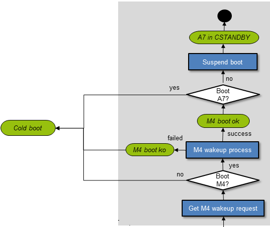
In such resets the Cortex®-M4 is always hold on reset, and only the ROM code on Cortex®-A7 is running. The behavior of the ROM code depends on value of bits MCU_BEN, MPU_BEN of RCC_MP_BOOTCR register.
- Cortex®-M4 wake up
If bit MCU_BEN of RCC_MP_BOOTCR register is set to 1, the ROM proceeds to Cortex®-M4 software wake up.
The ROM code wakes up Cortex®-M4 by releasing it from its "hold on reset" state.
- Cortex®-M4 software integrity check
- Before releasing Cortex®-M4 the ROM code can use backup registers to recover the Cortex®-M4 software integrity check value and compare it to the one computed on RETRAM.
- Note: if the device is closed, this check is mandatory.
- Cortex®-A7 wake up
The Cortex®-A7 software wake up consists in processing Secure boot.
The ROM will proceed to Cortex®-A7 software wake up in three cases:
- If M4 software wake up is not required (i.e. MCU_BEN=0)
- If M4 software wake up is required (i.e. MCU_BEN=0) but fails,
- If M4 software wake up is required (i.e. MCU_BEN=0), is processed successfully and MPU_BEN is also set to 1
- Cortex®-A7 returns to CStandby low power mode
If Cortex®-M4 software wake up is required (i.e. MCU_BEN=0), is processed successfully and MPU_BEN is set to 0, the ROM enters the Cortex®-A7 in CStandby low power modes.
7. RMA boot[edit source]
RMA boot allow a user to perform a Return Material Authorization (RMA).
- RMA Unlock
- The user can request to put a closed device in RMA state by configuring via Jtag the RMA unlock password in BSEC JTAG_IN register, which the ROM code compares to the password stored in OTP WORD 56
- RMA boot
- When the device is in unlocked for RMA : DFT tests are possible again, but without possibility to access any sensitive data stored in fuses by the user.
- RMA Relock
- The user can request to put a RMA device back in closed state by configuring via Jtag the RMA relock password in BSEC JTAG_IN register, which the ROM code compares to the password stored in OTP WORD 56
8. Configuration[edit source]
8.1. Boot device selection via the boot pins and OTP[edit source]
| BOOT pins | TAMP_REG[20] (Force Serial) |
OTP WORD 3 Primary boot source |
OTP WORD 3 Secondary boot source |
Boot source #1 | Boot source #2 if #1 fails |
Boot source if #2 fails |
|---|---|---|---|---|---|---|
| b000 | x (don't care) | x (don't care) | x (don't care) | Serial | - | - |
| b001 | != 0xFF | 0 (virgin) | 0 (virgin) | QSPI NOR | Serial | - |
| b010 | != 0xFF | 0 (virgin) | 0 (virgin) | e•MMC™ | Serial | - |
| b011 | != 0xFF | 0 (virgin) | 0 (virgin) | FMC NAND | Serial | - |
| b100 | x (don't care) | x (don't care) | x (don't care) | NoBoot | - | - |
| b101 | != 0xFF | 0 (virgin) | 0 (virgin) | SD-Card | Serial | - |
| b110 | != 0xFF | 0 (virgin) | 0 (virgin) | Serial | - | - |
| b111 | != 0xFF | 0 (virgin) | 0 (virgin) | QSPI NAND | Serial | - |
| != b100 | != 0xFF | Primary1 | 0 (virgin) | Primary1 | Serial | - |
| != b100 | != 0xFF | 0 (virgin) | Secondary1 | Secondary1 | Serial | - |
| != b100 | != 0xFF | Primary1 | Secondary1 | Primary1 | Secondary1 | Serial |
| != b100 | 0xFF | x (don't care) | x (don't care) | Serial | - | - |
1Primary and Secondary are fields of OTP WORD3.
8.2. OTP configuration[edit source]
The OTP are stored via BSEC internal peripheral.
8.2.1. OTP WORD 0[edit source]
| Bit | Name | Size | Value | Description |
|---|---|---|---|---|
| 31-7 | 25 bits | reserved | ||
| 6 | is_closed | 1 bit | Close state | |
| 0 | device is in open state, authentication is optional. | |||
| 1 | device is in close state, authentication is mandatory. | |||
| 5-0 | 6 bits | reserved |
8.2.2. OTP WORD 3[edit source]
| Bit | Name | Size | Value | Description |
|---|---|---|---|---|
| 31-30 | HSE_value | 2 bits | HSE value | |
| 0b00 | HSE is autodetected | |||
| 0b01 | HSE is 24 MHz | |||
| 0b10 | HSE is 25 MHz | |||
| 0b11 | HSE is 26 MHz | |||
| 29-27 | primary_boot_source | 3 bits | Primary boot source | |
| If different from zero, identifies primary source used for boot | ||||
| 0 | No primary boot source is defined | |||
| 1 | FMC NAND | |||
| 2 | QSPI NOR | |||
| 3 | e•MMC™ | |||
| 4 | SD | |||
| 5 | QSPI NAND | |||
| 26-24 | secondary_boot_source | 3 bits | Secondary boot source | |
| If different from zero, identifies secondary source used for boot | ||||
| 0 | No secondary boot source is defined | |||
| 1 | FMC NAND | |||
| 2 | QSPI NOR | |||
| 3 | e•MMC™ | |||
| 4 | SD | |||
| 5 | QSPI NAND | |||
| 23-16 | boot_source_disable | 8 bits | Disable boot source | |
| if different from zero each bit disables a boot source | ||||
| 0b00000001 | disable FMC NAND boot source | |||
| 0b00000010 | disable QSPI NOR boot source | |||
| 0b00000100 | disable e•MMC™ boot source | |||
| 0b00001000 | disable SD boot source | |||
| 0b00010000 | disable UART boot source | |||
| 0b00100000 | disable USB boot source | |||
| 0b01000000 | disable QSPI NAND boot source | |||
| 15-15 | no_data_cache | 1 bit | Data cache enable enabling | |
| If different from zero, data cache is not used by bootrom. | ||||
| 0 | Data cache is used by bootrom. | |||
| 1 | Data cache is not used by bootrom. | |||
| 14-7 | uart_intances_disabled | 8 bits | Uart instances disabled | |
| If different from zero each bit disables an UART instance. | ||||
| If all disable bits are set to 1 then all UARTs are enabled. | ||||
| 0b00000001 | reserved | |||
| 0b00000010 | disable USART2 | |||
| 0b00000100 | disable USART3 | |||
| 0b00001000 | disable UART4 | |||
| 0b00010000 | disable UART5 | |||
| 0b00100000 | disable UART6 | |||
| 0b01000000 | disable UART7 | |||
| 0b10000000 | disable USART8 | |||
| 6 | no_usb_dp_pullup | 1 bit | USB DP pullup enabling | |
| If different from zero, USB DP pull-up is not set | ||||
| 0 | USB DP pull-up is set | |||
| 1 | USB DP pull-up is not set | |||
| 5 | no_cpu_pll | 1 bit | PLL enabling | |
| If different from zero, PLL are not enabled | ||||
| 0 | PLLs for CPU/AXI are enable for cold boot | |||
| 1 | PLLs for CPU/AXI are not enable for cold boot | |||
| 4-3 | sd_if_id | 2 bits | SD Memory interface | |
| If different from zero, identifies the default instance to be used for memory boot | ||||
| 0 | Source is default one : SDMMC1 with default AFMux | |||
| 1 | SDMMC1 (uses non default AFmux defined in OTP) | |||
| 2 | SDMMC2 | |||
| 2-1 | emmc_if_id | 2 bits | e•MMC™ Memory interface | |
| If different from zero, identifies the default instance to be used for memory boot | ||||
| 0 | Source is default one : SDMMC2 with default AFMux | |||
| 1 | SDMMC1 | |||
| 2 | SDMMC2 (uses non default AFmux defined in OTP) | |||
| 0 | qspi_not_default_af | 1 bit | QSPI don’t use default AFmux | |
| 0 | QSPI uses default hard coded AFmux | |||
| 1 | QSPI uses AFmux defined in OTP |
8.2.3. OTP WORD 4 - Monotonic counter[edit source]
This is an anti rollback monotonic counter. On closed devices, the ROM code checks that it must be less or equal to the one stored in the image header.
| Bit | Name | Size | Value | Description |
|---|---|---|---|---|
| 31-0 | monotonic_val | 32 bits | Monotonic counter value | |
| Gives the value of monotonic counter | ||||
| 0b1xxxxxxxxxxxxxxxxxxxxxxxxxxxxxxx | Value of monotonic counter is 32 | |||
| 0b01xxxxxxxxxxxxxxxxxxxxxxxxxxxxxx | Value of monotonic counter is 31 | |||
| 0b001xxxxxxxxxxxxxxxxxxxxxxxxxxxxx | Value of monotonic counter is 30 | |||
| 0b0001xxxxxxxxxxxxxxxxxxxxxxxxxxxx | Value of monotonic counter is 29 | |||
| 0b00001xxxxxxxxxxxxxxxxxxxxxxxxxxx | Value of monotonic counter is 28 | |||
| 0b000001xxxxxxxxxxxxxxxxxxxxxxxxxx | Value of monotonic counter is 27 | |||
| 0b0000001xxxxxxxxxxxxxxxxxxxxxxxxx | Value of monotonic counter is 26 | |||
| 0b00000001xxxxxxxxxxxxxxxxxxxxxxxx | Value of monotonic counter is 25 | |||
| 0b000000001xxxxxxxxxxxxxxxxxxxxxxx | Value of monotonic counter is 24 | |||
| 0b0000000001xxxxxxxxxxxxxxxxxxxxxx | Value of monotonic counter is 23 | |||
| 0b00000000001xxxxxxxxxxxxxxxxxxxxx | Value of monotonic counter is 22 | |||
| 0b000000000001xxxxxxxxxxxxxxxxxxxx | Value of monotonic counter is 21 | |||
| 0b0000000000001xxxxxxxxxxxxxxxxxxx | Value of monotonic counter is 20 | |||
| 0b00000000000001xxxxxxxxxxxxxxxxxx | Value of monotonic counter is 19 | |||
| 0b000000000000001xxxxxxxxxxxxxxxxx | Value of monotonic counter is 18 | |||
| 0b0000000000000001xxxxxxxxxxxxxxxx | Value of monotonic counter is 17 | |||
| 0b00000000000000001xxxxxxxxxxxxxxx | Value of monotonic counter is 16 | |||
| 0b000000000000000001xxxxxxxxxxxxxx | Value of monotonic counter is 15 | |||
| 0b0000000000000000001xxxxxxxxxxxxx | Value of monotonic counter is 14 | |||
| 0b00000000000000000001xxxxxxxxxxxx | Value of monotonic counter is 13 | |||
| 0b000000000000000000001xxxxxxxxxxx | Value of monotonic counter is 12 | |||
| 0b0000000000000000000001xxxxxxxxxx | Value of monotonic counter is 11 | |||
| 0b00000000000000000000001xxxxxxxxx | Value of monotonic counter is 10 | |||
| 0b000000000000000000000001xxxxxxxx | Value of monotonic counter is 9 | |||
| 0b0000000000000000000000001xxxxxxx | Value of monotonic counter is 8 | |||
| 0b00000000000000000000000001xxxxxx | Value of monotonic counter is 7 | |||
| 0b000000000000000000000000001xxxxx | Value of monotonic counter is 6 | |||
| 0b0000000000000000000000000001xxxx | Value of monotonic counter is 5 | |||
| 0b00000000000000000000000000001xxx | Value of monotonic counter is 4 | |||
| 0b000000000000000000000000000001xx | Value of monotonic counter is 3 | |||
| 0b0000000000000000000000000000001x | Value of monotonic counter is 2 | |||
| 0b00000000000000000000000000000001 | Value of monotonic counter is 1 | |||
| 0b00000000000000000000000000000000 | Value of monotonic counter is 0 |
8.2.4. OTP WORD 5 to 7 - AFmux configuration[edit source]
| Bit | Field | Size | Value | Description |
|---|---|---|---|---|
| 31-28 | port1[3:0] | 4 bits | Bank id | |
| 0 | unused | |||
| 1 | Bank A | |||
| 2 | Bank B | |||
| 3 | Bank C | |||
| 4 | Bank D | |||
| 5 | Bank E | |||
| 6 | Bank FK | |||
| 7 | Bank G | |||
| 8 | Bank H | |||
| 9 | Bank I | |||
| 10 | Bank J | |||
| 11 | Bank K | |||
| 12 | Bank Z | |||
| 0b1111XXX | Invalid configuration | |||
| 27-24 | pin1[3:0] | 4 bits | 0-15 | Pin Id |
| 23-20 | afmux1[3:0] | 4 bits | 0-15 | AFmux value |
| 19-16 | mode0[3:0] | 4 bits | Pin Mode | |
| 0 | AF ; No Pull ; Low Speed | |||
| 1 | AF ; No Pull ; Medium Speed | |||
| 2 | AF ; No Pull ; High Speed | |||
| 3 | AF ; Pull Up ; Low Speed | |||
| 4 | AF ; Pull Up ; Medium Speed | |||
| 5 | AF ; Pull Up ; High Speed | |||
| 6 | AF ; Pull Down ; Low Speed | |||
| 7 | AF ; Pull Down ; Medium Speed | |||
| 8 | AF ; Pull Down ; High Speed | |||
| 9 | GPIO Output High | |||
| 10 | GPIO Output Low | |||
| 11 | GPIO Input | |||
| 12 | GPIO open drain ; No pull | |||
| 13 | GPIO open drain ; Pull Up | |||
| 14 | GPIO open drain ; Pull Down | |||
| 15 | GPIO analog mode | |||
| 15-12 | port0[3:0] | 4 bits | Bank id | |
| 0 | unused | |||
| 1 | Bank A | |||
| 2 | Bank B | |||
| 3 | Bank C | |||
| 4 | Bank D | |||
| 5 | Bank E | |||
| 6 | Bank FK | |||
| 7 | Bank G | |||
| 8 | Bank H | |||
| 9 | Bank I | |||
| 10 | Bank J | |||
| 11 | Bank K | |||
| 12 | Bank Z | |||
| 0b1111XXX | Invalid configuration | |||
| 8-Nov | pin0[3:0] | 4 bits | 0-15 | Pin Id |
| 4-Jul | afmux0[3:0] | 4 bits | 0-15 | AFmux value |
| 31-0 | pull0mode0[31:0] | 42 bits | Pin Pull Mode | |
| 0 | AF ; No Pull ; Low Speed | |||
| 1 | AF ; No Pull ; Medium Speed | |||
| 2 | AF ; No Pull ; High Speed | |||
| 3 | AF ; Pull Up ; Low Speed | |||
| 4 | AF ; Pull Up ; Medium Speed | |||
| 5 | AF ; Pull Up ; High Speed | |||
| 6 | AF ; Pull Down ; Low Speed | |||
| 7 | AF ; Pull Down ; Medium Speed | |||
| 8 | AF ; Pull Down ; High Speed | |||
| 9 | GPIO Output High | |||
| 10 | GPIO Output Low | |||
| 11 | GPIO Input | |||
| 12 | GPIO open drain ; No pull | |||
| 13 | GPIO open drain ; Pull Up | |||
| 14 | GPIO open drain ; Pull Down | |||
| 15 | GPIO analog mode; Pull down |
8.2.5. OTP WORD 9 - NAND configuration[edit source]
| Bit | Name | Size | Value | Description |
|---|---|---|---|---|
| 31-31 | nand_param_stored_in_otp | 1 bit | NAND parameters storage flag | |
| 0b0 | NAND parameters are not stored here in OTP and are available via an ‘ONFI’ compliant get parameter command. | |||
| 0b1 | NAND parameters are stored here in OTP | |||
| 30-29 | nand_page_size[1:0] | 2 bits | NAND page size | |
| 0 | Page size is 2 Kbytes | |||
| 1 | Page size is 4 Kbytes | |||
| 2 | Page size is 8 Kbytes | |||
| 3 | reserved | |||
| 28-27 | nand_block_size[1:0] | 2 bits | NAND block size | |
| 0 | Block size is 64 pages | |||
| 1 | Block size is 128 pages | |||
| 2 | Block size is 256 pages | |||
| 3 | reserved | |||
| 26-19 | nand_blocks_nb[7:0] | 8 bits | NAND number of blocks | |
| N | Number of blocks of NAND in unit of 256 blocks (= N * 256 blocks) | |||
| 18-18 | fmc_nand_width | 1 bit | FMC NAND width | |
| 0 | FMC NAND is 8 bits | |||
| 1 | FMC NAND is 16 bits | |||
| 17-15 | fmc_ecc_bit_nb[2:0] | 3 bits | FMC NAND number of ECC bits | |
| 0 | No setting. In case on ONFI NAND, means ‘use value defined in parameter table’ | |||
| 1 | 1 bit ECC per 512 bytes, Hamming code | |||
| 2 | 4 bit ECC per 512 bytes of data, BCH (Bose, Chaudhuri and Hocquenghem) code | |||
| 3 | 8 bit ECC per 512 bytes of data, BCH (Bose, Chaudhuri and Hocquenghem) code | |||
| 4 | on-die ECC | |||
| 14 | spinand_need_plane_select | 1 bit | SPI NAND need plane select | |
| 0 | SPI NAND plane select not needed. | |||
| 1 | SPI NAND plane select needed. | |||
| 13-4 | reserved | 11 bits | - | - |
| 3 | disable_ddr_power_optim | 1 bit | Disable DDR PLL switch off sequence | |
| 0 | DDR DLL switch off sequence enabled | |||
| 1 | DDR DLL switch off sequence disabled. | |||
| 2 | disable_hse_bypass_detect | 1 bit | Disable HSE bypass detection | |
| 0 | HSE bypass detection enabled. | |||
| 1 | HSE bypass detection disabled. | |||
| 1 | disable_hse_freq_detect | 1 bit | Disable HSE frequency autodetection | |
| 0 | HSE frequency autodetection enabled. | |||
| 1 | HSE frequency autodetection disabled. | |||
| 0 | disable_traces | 1 bit | Disable traces bit | |
| 0 | Bootrom trace are enabled. | |||
| 1 | Bootrom trace are disabled. |
8.2.6. OTP WORD 24 to 31 - Public Key Hash (PKH)[edit source]
OTP WORD 24 to 31 contain the SHA256 hash of (ECDSA algorithm id + ECDSA public key) where ECDSA algorithm id is 32-bit length and valid values are ‘1’ for P-256 NIST, or ‘2’ for Brainpool 256.
| OTP word | Bit | Field | Size | Description |
|---|---|---|---|---|
| 24 | 31-0 | pkh0[31:0] | 32 bits | Public Key Hash[31:0] |
| 25 | 31-0 | pkh1[31:0] | 32 bits | Public Key Hash[63:32] |
| 26 | 31-0 | pkh2[31:0] | 32 bits | Public Key Hash[95:64] |
| 27 | 31-0 | pkh3[31:0] | 32 bits | Public Key Hash[128:96] |
| 28 | 31-0 | pkh4[31:0] | 32 bits | Public Key Hash[159:128] |
| 29 | 31-0 | pkh5[31:0] | 32 bits | Public Key Hash[191:160] |
| 30 | 31-0 | pkh6[31:0] | 32 bits | Public Key Hash[223:192] |
| 31 | 31-0 | pkh7[31:0] | 32 bits | Public Key Hash[255:224] |
8.2.7. OTP WORD 56 - RMA password[edit source]
| Bit | Name | Size | Description |
|---|---|---|---|
| 31-30 | 2 bits | reserved | |
| 29-15 | rma_relock_passwd | 15 bits | Password required for RMA ReLock request |
| 14-0 | rma_passwd | 15 bits | Password required for RMA Unlock request |
9. Exported secure services[edit source]
The ROM exports authentication services to the following stages of the STM32MP15 secure boot.
10. Debug and error cases[edit source]
10.1. Debug and Error messages[edit source]
- PA13 management
- The ROM code uses PA13 pin to communicate some status. On STMicroelectronics boards, PA13 is connected to the red LED, as explained in LEDs and buttons on STM32 MPU boards article.
- in case of boot failure, the PA13 pin is set to low open-drain (i.e. red LED will light bright).
- During UART/USB boot, the PA13 pin will toggle open-drain at a rate of about 5 Hz until a connection is started (i.e. red LED will blink fast).
- With BOOT[2:0] = 0b100 (engineering boot, used for specific debug), PA13 will toggle opendrain at a rate of about 5 kHz (i.e. red LED will light weak).
- In all other cases, the PA13 is kept in it’s reset value, i.e. high-z until software setting.
- Traces
- During its execution, the ROM writes binary traces in memory.
- Traces can be downloaded from address range 0x2ffc1c00-0x2ffc2404
- In case of internal blocking error, the ROM code writes a uart log error at 9600bauds to PA13 pin.
10.2. Common debug and error cases[edit source]
- Memory Boot failure
- Secure boot flow always enters the serial boot loop during which the Error LED is blinking. Therefore, observing such blinking when Memory boot is required indicates that Memory boot failed.
- Security issue
- If the bootrom encounters a security issue, it stops immediately the secure boot and sets the Error LED to light bright.