| Coming soon |
This article explains what is ADC and how to use it through examples.
1. What is an analog to digital converter (ADC)?
The analog-to-digital converters allows the microcontroller to accept an analog value like a sensor output and convert the signal into the digital domain. In this article, we focus on the STM32L4 ADC.
1.1. Simplified block diagram
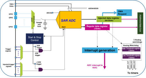
The figure below shows the general block diagram for each analog-to-digital converters embedded in the STM32L4.
1.2. ADC features in STM32L4x6 products
| ADC units | Up to 3 modules |
| Input channel | Up to 24 external channels (GPIOs), single/differential |
| Technology | 12-bit successive approximation |
| Conversion time | 188 nS, 5.33 Msamples/s (when fADC_CLK = 80 MHz) |
| Functional mode | Single, Continuous, Scan, Discontinuous, or Injected |
| Triggers | Software or external trigger (for Timers & IOs) |
| Special functions | Hardware oversampling, analog watchdogs |
| Data processing | Interrupt generation, DMA requests |
| Low-power modes | Deep power-down, auto delay, power consumption dependent on speed |
- High performance features
- Supports up to 5.33 mega samples per second of conversion which could be extended to 10Msamples/s (devices with dual ADC).
- Includes the oversampling hardware which accumulates data and then divides it without CPU.
- Flexible sequencer
- Auto-calibration to reduce offset
- Low Power features
- Deep power-down mode
- Auto-delayed conversion
- Power consumption depends on sampling time
- Conversion Speeds
- ADC needs minimum 2.5ADC_CLKs for sample period and 12.5ADC_CLKs for conversion (12-bit).
- 80 MHz maximum clock with a 15 cycle results in 5.33 Msamples/s
- Speed up by low resolution
- Programmable sampling time
- Flexible clock selection
1.3. ADC Conversion Modes
AD converter supports several conversion modes: Single mode, which converts only one channel, in single-shot or continuous mode. Scan mode, which converts a complete set of pre-defined programmed input channels, in single-shot or continuous mode. Discontinuous mode, converts only a single channel at each trigger signal from the list of pre-defined programmed input channels.
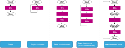
There are several functional modes which will be explained in details in the Reference Manual.
2. Configuring ADC to measure the DAC
2.1. Objectives
- Learning how to set up the ADC with DMA in STM32CubeMX.
- Generating code in STM32CubeMX and using HAL functions.
- Creating a simple application to start the ADC and measure the DAC.
2.2. Create the project in STM32CubeMX
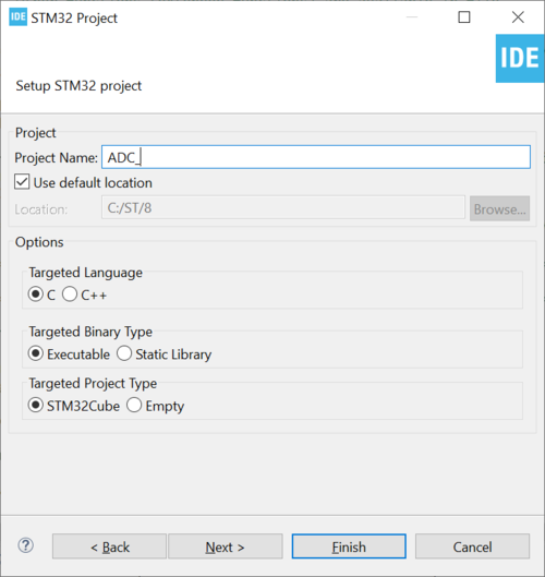
2.1. Creating the project in STM32CubeIDE
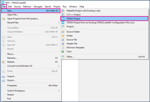
- File > New > STM32 Project in main panel.
 .
.
This example uses the NUCLEO-L476RG board.
- Select NUCLEO-L476RG board using Board selector as shown in the figure below:
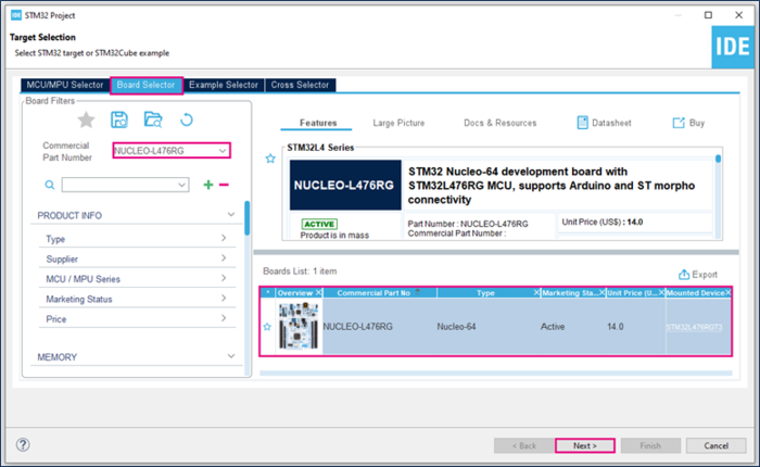
If you did not download the STM32L476 Cube library, it will automatically be downloaded. This can take some time.
- Save the project:
2.2. Configuring ADC & DAC
2.2.1. Configuring DAC
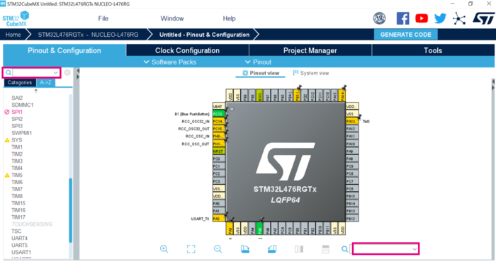
- Search for DAC1 in the left search field.
We will use PA5 as the DAC's output.
As it is configured as GPIO Output by default, we need to reset it first.
- Search for PA5 in the bottom right search field, then click Reset_State.
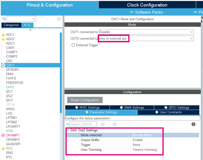
- Connect OUT2 only to external pin. Notice how PA5 is automatically set to DAC1_OUT2 on the pinout view.
- Parameter Settings should be set up as in the below example: normal mode, buffer enabled and no trigger.
2.2.2. Configuring ADC
Configure ADC the following settings:
- Asynchronous clock mode div by 1
- Resolution 12bits
- Right alignment
- Software trigger
- sampling time for CH6 (92.5cycles)
- DMA Continuous requests
2.2.3. Configuring DMA
The ADC conversion values will be transferred into memory by DMA controller.
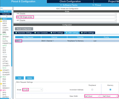
2.3. Generating the project and editing main.c
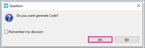
- Click Ctrl+S to generate the project:
- Edit main.c:
/* USER CODE BEGIN PV */
uint32_t value_adc;
uint32_t value_dac=0;
/* USER CODE END PV */
/* USER CODE BEGIN 2 */
HAL_DAC_Start(&hdac1,DAC_CHANNEL_2);
HAL_DAC_SetValue(&hdac1, DAC_CHANNEL_2, DAC_ALIGN_12B_R, value_dac);
HAL_ADCEx_Calibration_Start(&hadc1, ADC_SINGLE_ENDED);
HAL_ADC_Start_DMA(&hadc1,(uint32_t*)&value_adc,1);
/* USER CODE END 2 */
/* USER CODE BEGIN 3 */
while (1)
{
HAL_DAC_SetValue(&hdac1, DAC_CHANNEL_2, DAC_ALIGN_12B_R, value_dac);
value_dac++;
if(value_dac>4095){
value_dac=0;
}
HAL_Delay(20);
HAL_ADC_Start(&hadc1);
HAL_Delay(10);
}
/* USER CODE END 3 */
- Explanation
Inside the if conditional statement, we check if dac_value is lower than 4095 (0xFFF) which is the maximum output value for a 12-bit resolution DAC:
- If the value is lower than the maximum value, it is incremented.
- If not, it is reset back to zero.
- Then, we add a 1ms delay in order to have a stable output DAC value.
We will sweep through all the ADC output possible values in roughly 80ms and then it resets to zero restarting the process all over again
As the ADC was configured with software trigger, we need to start it in our code.
After the end of each conversion, it will automatically invoke a DMA transfer to memory.
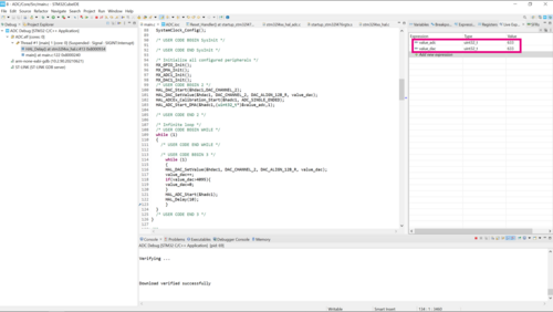
ADC and DAC have similar values, to verify remove PA1 – PA5 jumper.
This will be running in the infinite loop. Therefore, the code will sweep through all the possible DAC output values, and then reset it to zero restarting the process all over again.
2.4. Compiling and flashing
3. Building and measure a simple signal generator
- Put jumper on PA1 - PA5 pins to connect DAC output to ADC input. The result is as follows
- Explore further possibilities such as:
- How to get the best ADC accuracy in STM32 microcontrollers [1]
4. References
[[category:Getting_started_with_STM32_system_peripherals | 70]]
