1. Article purpose[edit | edit source]
This article explains how to configure the TF-A MTD frameworks:
- SPI NOR
- SPI NAND
- SPI MEM
- FMC NAND
- HYPERFLASH NOR
These frameworks represent the memory-access organisation.
They use two different configurations:
- Device tree configuration
- Boot device configuration[1]
If the peripheral is assigned to another execution context, refer to How to assign an internal peripheral to an execution context article for guidelines on peripheral assignment and configuration.
2. Framework overview[edit | edit source]
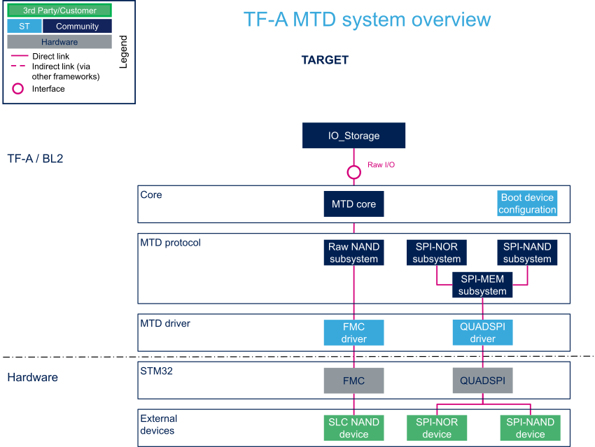
2.1. On STM32MP1 series[edit | edit source]
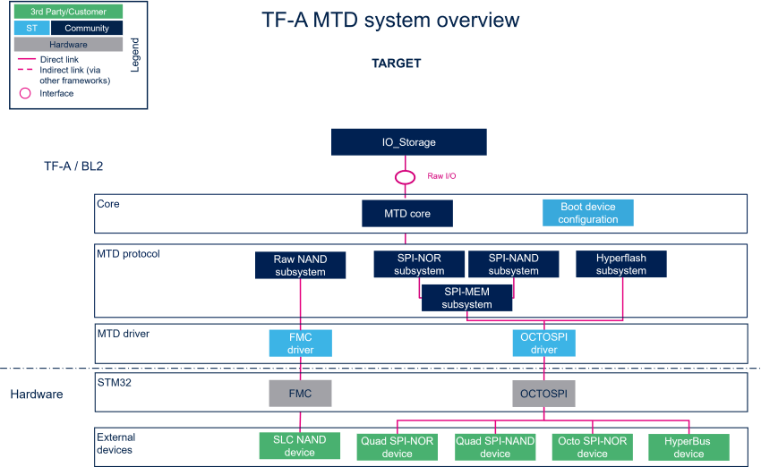
2.2. On STM32MP2 series[edit | edit source]
2.3. Components description[edit | edit source]
- IO_Storage. The IO storage provides an abstraction layer to access storage devices.
- Boot device configuration[1]. The Boot device configuration is a platform specific add-on to manage Flash memory settings.
- MTD core. The MTD core provides an abstraction layer for raw Flash memories.
- Raw NAND subsystem. The Raw NAND protocol is used in the MTD subsystem for interfacing NAND Flash memories.
- SPI-MEM subsystem. The SPI-MEM protocol is used in the MTD subsystem for interfacing all kinds of SPI memories (NORs, NANDs).
- SPI-NAND subsystem. The SPI-NAND protocol is used in the MTD subsystem for interfacing SPI NAND Flash memories.
- SPI-NOR subsystem. The SPI-NOR protocol is used in the MTD subsystem for interfacing SPI NOR Flash memories.
- CFI subsystem. The Common Flash Interface protocol is used in the MTD subsystem for interfacing HYPERFLASH NOR Flash memories.
- FMC driver / FMC (Hardware) . Please refer to the FMC internal peripheral.
- QUADSPI driver / QUADSPI (Hardware). Please refer to the QUADSPI internal peripheral.
- OCTOSPI driver (Kernel space) / OCTOSPI (Hardware). Please refer to the OCTOSPI internal peripheral.
- HyperBus driver (Kernel space) / OCTOSPI (Hardware). Please refer to the OCTOSPI internal peripheral.
3. DT configuration[edit | edit source]
This hardware description is a combination of the STM32 microprocessor device tree files (.dtsi extension) and board device tree files (.dts extension). See the Device tree for an explanation of the device tree file split.
STM32CubeMX can be used to generate the board device tree. Refer to How to configure the DT using STM32CubeMX for more details.
4. Raw NAND Flash memory[edit | edit source]
4.1. Raw NAND DT configuration[edit | edit source]
For the DT bindings, refer to FMC device tree configuration.
4.2. Raw NAND device configuration[edit | edit source]
Raw NAND access uses the raw NAND framework. Some additional parameters are required by the raw NAND framework to address the memory:
- the page size
- the block size
- the number of blocks per device
- the bus width (8 or 16 bits)
- the ECC algorithm (HW BCH8/BCH4/Hamming algorithms are available). The default ECC used is ECC NONE (no error correction).
Some memories are ONFI[2] compliant. In that case, the required parameters can be directly read from the parameter description table.
For the others, the user must correctly fill-out the OTP fuses dedicated for NAND.
- For STM32MP15x lines
 OTP9 should be filled, see STM32MP15 OTP mapping.
 - For STM32MP13x lines
 OTP9 and/or OTP10 should be filled, see STM32MP13 OTP mapping.
 - For STM32MP25x lines
 OTP16 and/or OTP20 should be filled, see STM32MP25 OTP mapping.
4.2.1. Raw NAND examples (STM32MP1 series)[edit | edit source]
- ONFI raw NAND with ECC override (default from parameter table is BCH4, force to BCH8).
OTP Word 9 : 0x18000
| Use OTP | Page size | Block size | Block numbers (N * 256) | Width | ECC | ||||||||||||||||||||||||||
|---|---|---|---|---|---|---|---|---|---|---|---|---|---|---|---|---|---|---|---|---|---|---|---|---|---|---|---|---|---|---|---|
| 0 | 0 | 0 | 0 | 0 | 0 | 0 | 0 | 0 | 0 | 0 | 0 | 0 | 0 | 0 | 1 | 1 | 0 | 0 | 0 | 0 | 0 | 0 | 0 | 0 | 0 | 0 | 0 | 0 | 0 | 0 | 0 |
- 8-bit raw NAND (page size: 4 Kbytes, block size: 256 Kbytes, device size: 1024 Mbytes, ECC requirement: BCH4)
OTP Word 9 : 0xA0810000
| Use OTP | Page size | Block size | Block numbers (N * 256) | Width | ECC | ||||||||||||||||||||||||||
|---|---|---|---|---|---|---|---|---|---|---|---|---|---|---|---|---|---|---|---|---|---|---|---|---|---|---|---|---|---|---|---|
| 1 | 0 | 1 | 0 | 0 | 0 | 0 | 0 | 1 | 0 | 0 | 0 | 0 | 0 | 0 | 1 | 0 | 0 | 0 | 0 | 0 | 0 | 0 | 0 | 0 | 0 | 0 | 0 | 0 | 0 | 0 | 0 |
- 16-bit raw NAND (page size: 8 Kbytes, block size: 512 Kbytes, device size: 2048 Mbytes, ECC requirement: ON-DIE)
OTP Word 9 : 0xc0860000
| Use OTP | Page size | Block size | Block numbers (N * 256) | Width | ECC | ||||||||||||||||||||||||||
|---|---|---|---|---|---|---|---|---|---|---|---|---|---|---|---|---|---|---|---|---|---|---|---|---|---|---|---|---|---|---|---|
| 1 | 1 | 0 | 0 | 0 | 0 | 0 | 0 | 1 | 0 | 0 | 0 | 0 | 1 | 1 | 0 | 0 | 0 | 0 | 0 | 0 | 0 | 0 | 0 | 0 | 0 | 0 | 0 | 0 | 0 | 0 | 0 |
5. SPI NAND flash memory[edit | edit source]
5.1. SPI NAND DT configuration[edit | edit source]
5.1.1. On STM32MP1 series[edit | edit source]
For the DT bindings, refer to the QUADSPI device tree configuration.
5.1.2. On STM32MP2 series[edit | edit source]
For the DT bindings, refer to the OCTOSPI device tree configuration.
5.2. SPI NAND device configuration[edit | edit source]
SPI NAND and SPI MEM frameworks are used to address such memories.
5.2.1. SPI NAND framework[edit | edit source]
SPI NAND framework requires additional parameters:
- the page size
- the block size
- the number of blocks per device
- the number of planes per device.
These parameters must be correctly filled out by the user in OTP fuses.
- For STM32MP15x lines
 OTP9 should be filled, see STM32MP15 OTP mapping.
 - For STM32MP13x lines
 OTP9 and/or OTP10 should be filled, see STM32MP13 OTP mapping.
 - For STM32MP25x lines
 OTP16 and/or OTP20 should be filled, see STM32MP25 OTP mapping.
By default, the READ FROM CACHE x1 command is used (opcode: 0x03). It is possible to override this command in the platform configuration to improve memory-access performance.
Some memory manufacturers require to enable the Quad Enable feature to support quad read command. It can be done by adding the flag SPI_NAND_HAS_QE_BIT.
5.2.2. SPI NAND example[edit | edit source]
- SPI NAND (page size: 2 Kbytes, block size: 128 Kbytes, device size: 256 Mbytes, 2 planes)
OTP Word 9 : 0x80404000
| Use OTP | Page size | Block size | Block numbers (N * 256) | Not Used | Not Used | 2 Planes | |||||||||||||||||||||||||
|---|---|---|---|---|---|---|---|---|---|---|---|---|---|---|---|---|---|---|---|---|---|---|---|---|---|---|---|---|---|---|---|
| 1 | 0 | 0 | 0 | 0 | 0 | 0 | 0 | 0 | 1 | 0 | 0 | 0 | 0 | 0 | 0 | 0 | 1 | 0 | 0 | 0 | 0 | 0 | 0 | 0 | 0 | 0 | 0 | 0 | 0 | 0 | 0 |
- Update the READ FROM CACHE x1 command to use the READ FROM CACHE x4 command (opcode: 0x6B) defined in platform file[1]
device->spi_read_cache_op.cmd.opcode = SPI_NAND_OP_READ_FROM_CACHE_4X;
device->spi_read_cache_op.cmd.buswidth = SPI_MEM_BUSWIDTH_1_LINE;
device->spi_read_cache_op.addr.nbytes = 2U;
device->spi_read_cache_op.addr.buswidth = SPI_MEM_BUSWIDTH_1_LINE;
device->spi_read_cache_op.dummy.nbytes = 1U;
device->spi_read_cache_op.dummy.buswidth = SPI_MEM_BUSWIDTH_1_LINE;
device->spi_read_cache_op.data.buswidth = SPI_MEM_BUSWIDTH_4_LINE;
device->spi_read_cache_op.data.dir = SPI_MEM_DATA_IN;
- Set SPI_NAND_HAS_QE_BIT flag if it is required by the memory.
device->flags |= SPI_NAND_HAS_QE_BIT;
6. MTD Framework - NAND specific[edit | edit source]
6.1. NAND error management[edit | edit source]
The TF-A BL2 MTD framework implements a retry mechanism link to NAND specification.
It allows to skip some bad blocks when loading binaries or switching to a backup partition if uncorrectable error is detected.
A PLATFORM_MTD_MAX_PART_SIZE defines the partition size to find a binary and its backups in the plat/st/common/include/stm32mp_io_storage.h . It can be increased or decreased depending the binary size (i.e FIP size and its backups).
On some specific NAND devices with ON-DIE ECC, an uncorrectable error is not checked and may result on a incomplete binary loaded with a boot failure.
| It is strongly recommended to use the Trusted Board Boot when using NAND memories to control the binary integrity loaded and avoid issues. |
6.2. Firmware Update[edit | edit source]
In case of Firmware update feature enabled, specific FIP offset for A (STM32MP_NAND_FIP_A_OFFSET) and B partition (STM32MP_NAND_FIP_B_OFFSET) are fixed in the plat/st/common/include/stm32mp_io_storage.h . They must be adapted depending on the FIP size loaded. They must be aligned with the PLATFORM_MTD_MAX_PART_SIZE previously explained.
7. SPI NOR Flash memory[edit | edit source]
7.1. SPI NOR DT configuration[edit | edit source]
7.1.1. On STM32MP1 series[edit | edit source]
For the DT bindings, refer to the QUADSPI device tree configuration.
7.1.2. On STM32MP2 series[edit | edit source]
For the DT bindings, refer to the OCTOSPI device tree configuration.
7.2. SPI NOR device configuration[edit | edit source]
SPI NOR and SPI MEM frameworks are used to address such memories.
7.2.1. SPI NOR framework[edit | edit source]
SPI NOR framework requires additional parameter:
- Device size
This parameter needs to be defined in the platform configuration file[1].
By default, the READ command is used (opcode: 0x03). It is possible to override this command in the platform configuration to improve memory-access performance .
7.2.2. SPI NOR example[edit | edit source]
- SPI NOR (device size: 64 Mbytes)
device->size = SZ_64M; --> Device size
- Update the READ command to use QREAD command (opcode: 0x6B) defined in platform file[1]
	device->read_op.cmd.opcode = SPI_NOR_OP_READ_1_1_4;
	device->read_op.cmd.buswidth = SPI_MEM_BUSWIDTH_1_LINE;
	device->read_op.addr.nbytes = 3U;
	device->read_op.addr.buswidth = SPI_MEM_BUSWIDTH_1_LINE;
	device->read_op.dummy.nbytes = 1U;
	device->read_op.dummy.buswidth = SPI_MEM_BUSWIDTH_1_LINE;
	device->read_op.data.buswidth = SPI_MEM_BUSWIDTH_4_LINE;
	device->read_op.data.dir = SPI_MEM_DATA_IN;
8. HYPERFLASH NOR Flash memory on STM32MP2 series[edit | edit source]
8.1. HYPERFLASH NOR DT configuration[edit | edit source]
For the DT bindings, refer to the OCTOSPI device tree configuration.
8.2. HYPERFLASH NOR device configuration[edit | edit source]
HYPERFLASH framework is used to address such memories.
8.2.1. HYPERFLASH NOR framework[edit | edit source]
HYPERFLASH NOR framework requires additional parameter:
- Device size
This parameter needs to be defined in the platform configuration file[1].
8.2.2. HYPERFLASH NOR example[edit | edit source]
- HYPERFLASH NOR (device size: 64 Mbytes)
device->size = SZ_64M; --> Device size
9. How to configure the DT using STM32CubeMX[edit | edit source]
The STM32CubeMX tool can be used to configure the STM32MPU device and get the corresponding platform configuration device tree files.
The STM32CubeMX might not support all the properties described in your device DT bindings (see the above Raw NAND, SPI NAND, SPI NOR or HYPERFLASH NOR dedicated DT configuration paragraphs). If so, the tool inserts user sections in the generated device tree. These sections can then be edited to add some properties, and they are preserved from one generation to another. Refer to the STM32CubeMX user manual for further information.
10. References[edit | edit source]
Please refer to the following links for additional information:

